Hi, Experts:
I am struggling with the PLL phase noise simulation with clock design tool for LMK04828. Kindly, can you please take some time to check if there any errors during my simulation?
I simulate the PLL1 phase noise curves by typing below in clock design tool:
The datasheet says the PN1Hz and PN10KHz of PLL1 as below:
I take PLL1_CP_GAIN = 1550uA, and do the simulation.
Assuming my reference clock for PLL1 is 122.88MHz, PFD frequency is 15.36MHz, VCXO frequency is 122.88MHz.
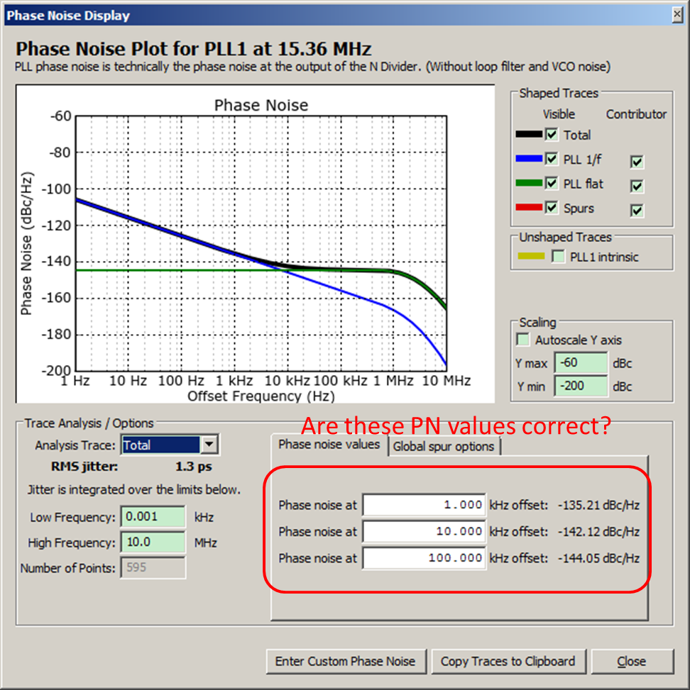
- I can get the Flat Noise at PLL1 output as below:
Lpll_flat(f) = PN1HZ + 20log(N) + 10log(fpdx) = -223 + 20*log(8) + 10log(15.36MHz) = -133.07dBc/Hz
Flat noise at PLL1 output will improved by 10*logfpdx if we increase the PFD frequency.
2. I also can get the Flicker noise at 10KHz offset at PLL1 output as below:
Lpll_flicker(10KHz) = PN10KHz + 20log(Fout/1GHz) +20*log(N) = -118 + 20*log(0.01536/1) + 20*log(8)= -136.21dBc/Hz
Since the flicker noise has a slope of -10dB/dec. I can get the flicker noise at PLL1 output across frequency as below:
|
Offset(KHz) |
Flicker noise @PLL1 output PN(dBc/Hz) |
|
0.01 |
-106.2103759 |
|
0.1 |
-116.2103759 |
|
1 |
-126.2103759 |
|
10 |
-136.2103759 |
|
100 |
-146.2103759 |
|
1000 |
-156.2103759 |
|
10000 |
-166.2103759 |
The flicker noise keeps constant independent of the PFD frequency.
3. Hence, add flicker noise and flat noise together, and I can get the total PLL1 noise at the VCXO output as below:
|
Offset(KHz) |
PN(dBc/Hz) |
|
0.01 |
-106.201444 |
|
0.1 |
-116.1218725 |
|
1 |
-125.3973442 |
|
10 |
-131.3549013 |
|
100 |
-132.8683031 |
|
1000 |
-133.0532444 |
|
10000 |
-133.0721791 |
Above is my calculation in theory for the expected PLL1 noise contribution at PLL1 VCXO output.
4. Start the simulation
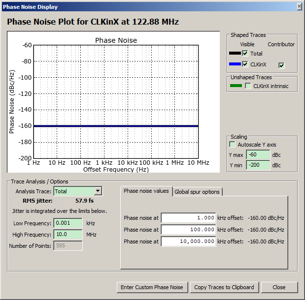
a. To exclude the reference phase noise contribution, I set the reference phase noise to -160dBc/Hz
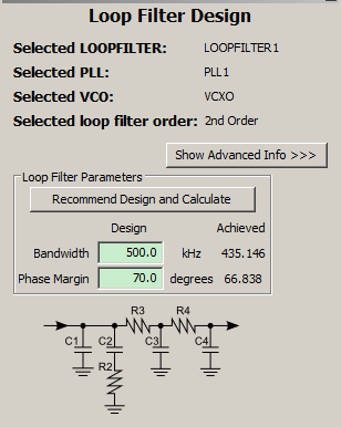
b. Set the PLL1 loop bandwidth large enough (~500KHz) to help me check the PLL1 phase noise more clearly
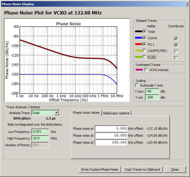
c. On the other hand, I disable the phase noise contribution from VCXO and loop filter:
While, I find there is a huge gap between the simulation result and calculated result at the VCXO (PLL1 output):
|
Offset(KHz) |
Calculated PN(dBc/Hz) |
Simulated PN(dBc/Hz) |
|
0.01 |
-106.201444 |
|
|
0.1 |
-116.1218725 |
|
|
1 |
-125.3973442 |
-117.15 |
|
10 |
-131.3549013 |
-124.06 |
|
100 |
-132.8683031 |
125.99 |
|
1000 |
-133.0532444 |
|
|
10000 |
-133.0721791 |
|
I am thinking the PLL1 phase noise (flicker noise and flat noise) may have some problem. Could you kindly help me to check my calculation to see if there is any problem? Thank you in advance.
Thanks
Yarn


