This thread has been locked.

If you have a related question, please click the "Ask a related question" button in the top right corner. The newly created question will be automatically linked to this question.

LM555: Duty cycle shifts as a function of output load

Part Number: LM555
Other Parts Discussed in Thread: TLC555,

Continuation of troubleshooting from this post: https://e2e.ti.com/support/clocks/f/48/t/650131. The problem in that post was solved with the reduction of output capacitance to remove chip heating.

The duty cycle of the 555 timer's output is changing based on the output load. With approximately 72.5ohms (measured), the duty cycle is at 100%. With 120ohms the duty cycle decreases to ~80%. I am concerned the 555 timer has sustained damage from previous troubleshooting and operation, but am looking for any other explanation as to why the loading can affect the duty cycle of the chip, short of damage.

Having probed the Trigger and Threshold pins, the voltage at those pins is not rising beyond ~6V, and the control voltage is at ~6.5V -> so the voltage thresholds are okay, but the trigger/threshold is not charging up beyond the 6.6V needed to trip the trigger.

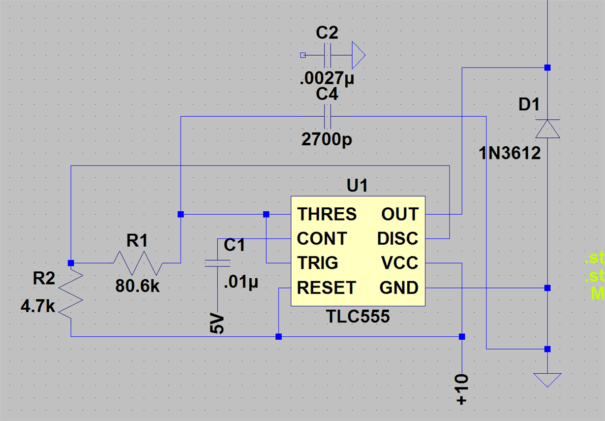
I apologize for the LTSpice schematic, but I am still learning TI-Tina and this was faster for me right now. Simulation does not show a problem or frequency shift with different loads, though admittedly the only simulation chip available is the TLC555, not the LM555.

I am continuing to troubleshoot the problem in the lab, and will try a chip swap to see if the operation changes.

  • Will,

    Can you try to attach the schematic again? The link did not work.
    Load on pin 3 should not change the timing unless pin 3 is part of the timing (instead on pin 7) or VCC is affected by the load.
  • Change in load is from ~72ohms series w/ 15mH (edited from 3.2mH) inductance (non functional), to ~150ohms w/ 15mH inductance (operating as designed), and on the way the duty cycle contracts from 100% until reaching the desired ~50% duty cycle.

    Ron, let me know if the schematic didn't come through. I tried conventional attachments over import screenshot.

  • Will,

    At 72 ohm load, the output current is too high for the TLC555 at 10V. The device might overheat.
    C1 is terminated to 5V instead of ground. So noise on 5V will affect timing thresholds.
    I don't see the load however I assume it is connected to 10V also.

    Regardless, I would still expect a 50% output although the VOL may be very high.
    Start with a new TLC555 installed.
  • Hi Ronald! Let me summarize as much as I can do:
    I just received the new TLC555 yesterday. I will try to swap the components and run tests, but I've been sidetracked onto more critical issues, given that the issue appears to be isolated and fixed:
    As far as I can tell, the issue is with mismatched impedances between the 555 timer and the load resolver. The load impedance of the resolver is pushing and pulling on the 555 timer, which is causing erroneous behavior with the timer. My evidence for this is:

    1. Changing the shielding of the cable the 555 timer's signal goes out of; between terminated at both ends, terminated at one end, and terminated at neither end changes the duty cycle pulling, frequency shifting, and whether or not the device locks up into a permanent high or low state. I have verified, both by design and by physically measuring, that the shield is isolated from the resolver (load) and input AND I have verified that I'm not introducing a short into the cable line by changing the shield around (so no ground loops or active signals shorted into the shield GND). What the shield changes are doing is changing the cable impedance (it's shielded twisted pair, not matched impedance shielded twisted pair).
    2. In order to fix the problem, a small capacitor (.22uF) was added to the output of the 555 timer. This balances out the output impedance seen by the timer, effectively forming a pi network with .22uF input, 15mH + 72ohm bridge impedance, and 11uF output capacitance. Note that this is far less than the 1uF that was there on the 555's output previously, which causes too much current to be drawn out of the 555 timer, and was causing a previous problem that I recall you helping me with ; )
    3. For a test, I fed the output of the 555 to a 200ohm resistor connected to the base of an NPN, with the collector of the NPN tied to 10V and the emitter being the new output. Basically, it's a driver, but without the complementary PNP to pull the output low, it just relies on the load bleeding off the output fast enough instead of actively pulling the output low. And that did the trick: the output of the 555 is perfectly stable, even under heating, and the output of the NPN driver is stable as well, being better matched to drive the inductive output load directly from +10V.
    4. Additional decoupling, even both ceramic and midling ESR tantalum caps up to 300uF on the input to the 555 timer provided no benefits to solving the problem -> suggests to me this is the equivalent impedance of the 555 timer's internal BJT output drivers, and independent of reasonable decoupling.
    5. Noise was measured on the 5V line, and 10V line. The noise is down in the 10's of mV range, which could cause a small amount of frequency and duty cycle drift, but not on par with up to the 50% change observed.

    Thanks for your help, Ronald! I'm going to leave this issue open, and as I get more time I'm going to install the TLC555 to see if a CMOS device's output impedance is sufficient to make the problems go away without requiring impedance compensation OR a driver.

    -Will
  • Will,

    Thanks for the additional information. I would call the issue 'overloading' opposed to calling it 'impedance matching'. I do like the idea of letting the NPN do the brunt of the current driving. I am glad that you are making progress.