Because of the holidays, TI E2E™ design support forum responses will be delayed from Dec. 25 through Jan. 2. Thank you for your patience.

This thread has been locked.

If you have a related question, please click the "Ask a related question" button in the top right corner. The newly created question will be automatically linked to this question.

LMK03033: LMK03033 configuration problem

Part Number: LMK03033

Good day! I have a problem with LMK03033 configuration. I used the following registers (verilog):

32'h80000000,
 32'h00030300,
 32'h00030301,
 32'h00030302,
 32'h00030303,
 32'h00030304,
 32'h00030305,
 32'h00030306,
 32'ha0032a09,
 32'h0082800B,
 32'h28E000D,
 32'h1840020E,
 32'hCC00180F

At the output of the device, I see 105 MGh and Lock Detect is't working, when at the input is 56 MGh.

The attachment contains circuit and timing diagram during programming.

UFSS_Conditioner_COPY.pdf

  • And additional question. Is there any way to read device registers?
  • Dear Nokolay,

    I recommend you follow the programming sequence in section 7.1 of the D/S. that sequence start a with a reset. It appears you are missing that steps at least.

    I also do not see a way to read back the registers.

    I hope this helps.

    Regards, Simon.
  • Simon, thank you for the answer.


    If I correctly understood the description, then the first word in the sequence is a reset (32'h80000000). Or this is not?

    This is from datasheet:

    The recommended programming sequence involves programming R0 with the reset bit set (RESET = 1) to
    ensure the device is in a default state. It is not necessary to program R0 again, but if R0 is programmed
    again, the reset bit is programmed clear (RESET = 0). Registers are programmed in order with R15 being
    the last register programmed. An example programming sequence is shown below.
  • Dear Nicolay,

    I recommend you use TiCS PRO software we provide on ti.com to check a defaults sequence and how it matches with the actual configuration. Check the window in the bottom left of the software, you will see the programming sequence when you type CTRL-C.

    You can also try the default configurations in TiCS PRO as a starting point for your own use case.

    Finally, TiCS PRO does NOT need to be connected to a device to use it.

    Let me know if you have more questions.

    Regards, Simon.
  • I tried this sequence, but the device does not work correctly.

    32'h8000_0100,

    32'h8000_0100,

    32'h0000_0100,

    32'h0003_0301,

    32'h0000_0102,

    32'h0000_0103,

    32'h0000_0104,

    32'h0000_0105,

    32'h0000_0106,

    32'h0000_0107,

    32'h1000_0908,

    32'ha003_2a09,

    32'h0082_000B,

    32'h028E_00aD,

    32'h0803_020E,

    32'hCC00_180F

    LD is't working and 121 MHz at the output (expected 112 MHz)

    Is there something wrong in the timing diagram?

  • Dear Nicolay,

    your timing diagram looks fine. Are you able to see it on a scope with single capture?

    Regards, Simon.
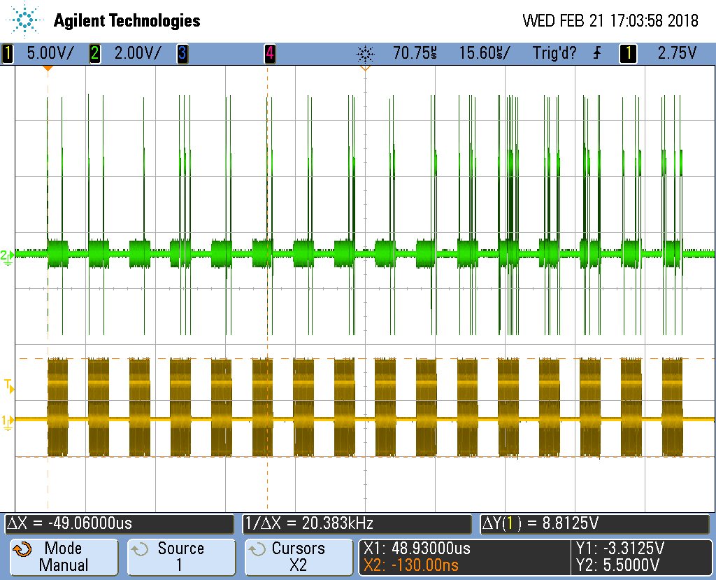
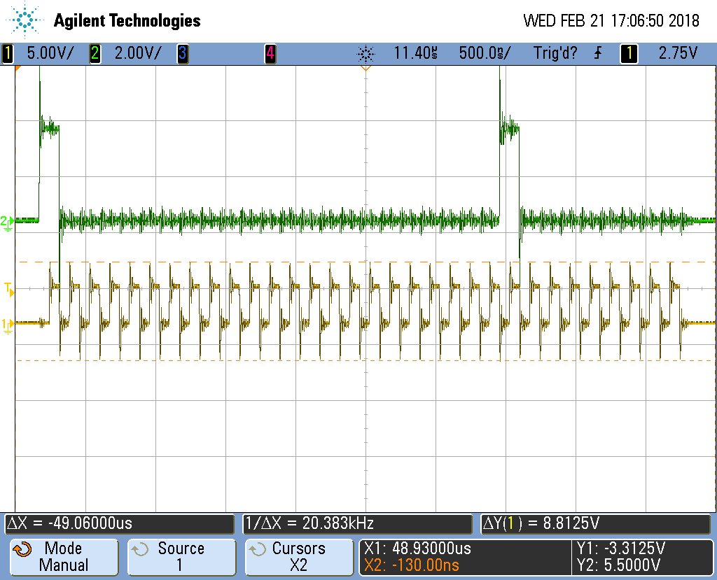
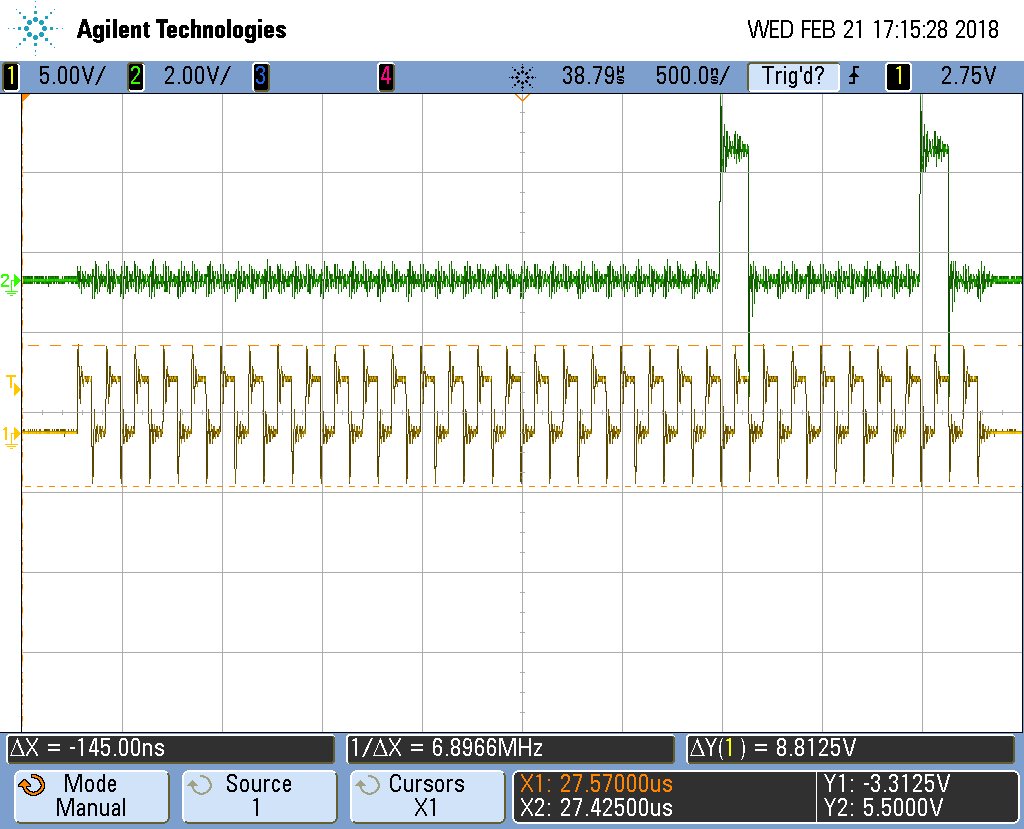
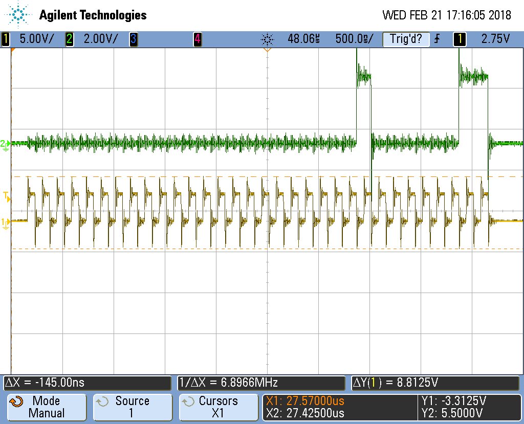
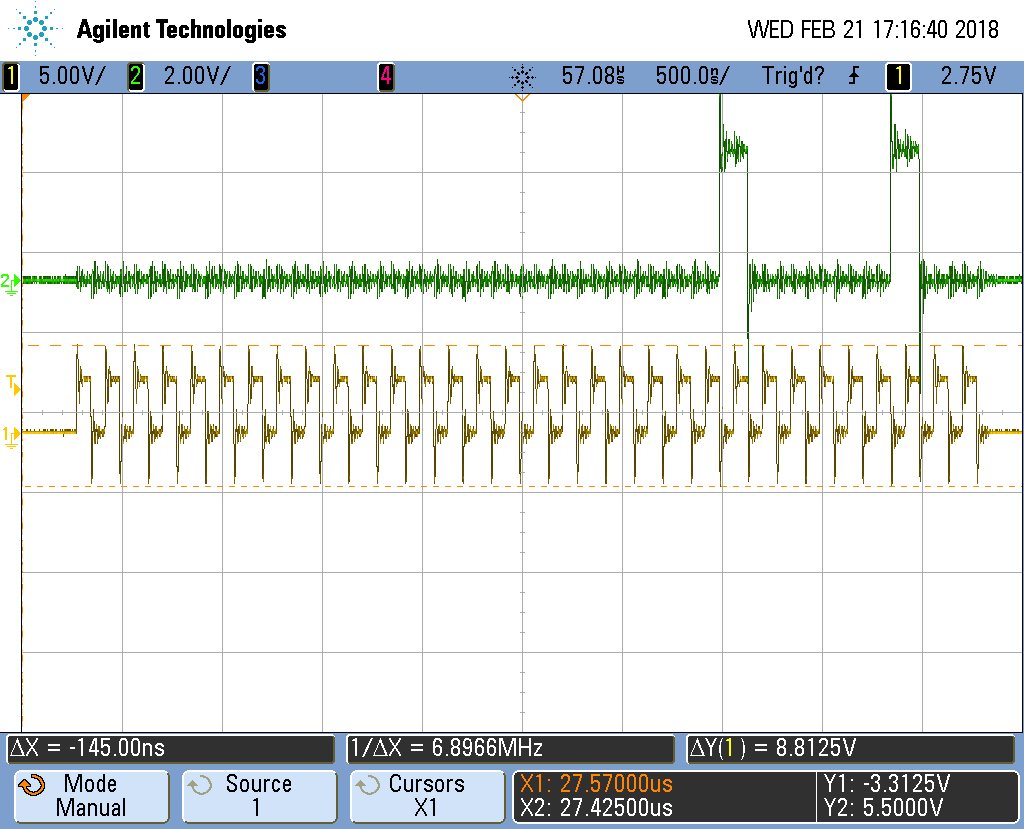
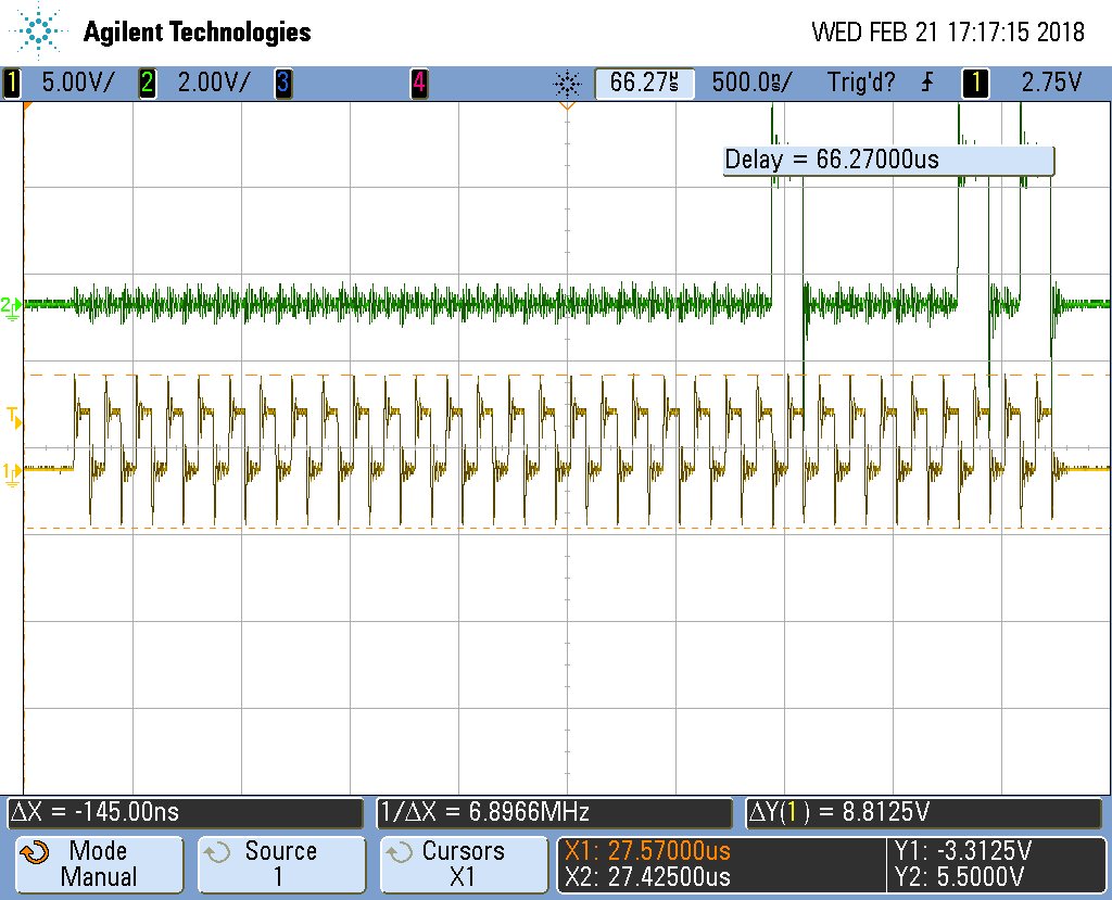
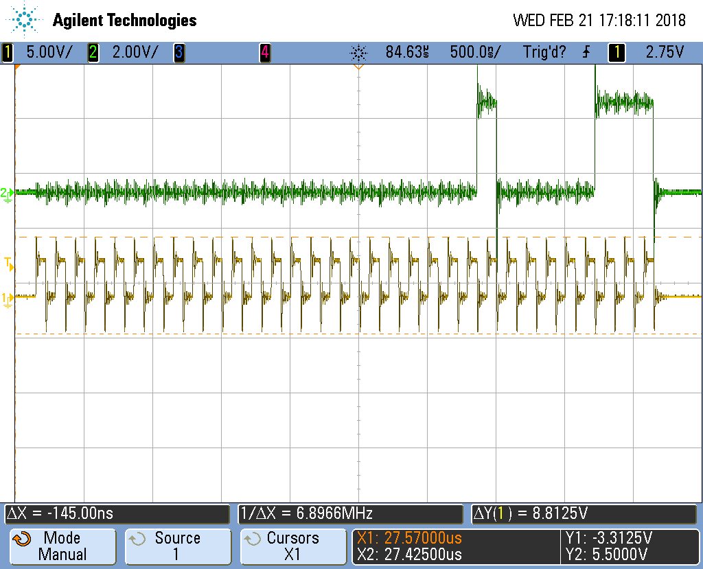
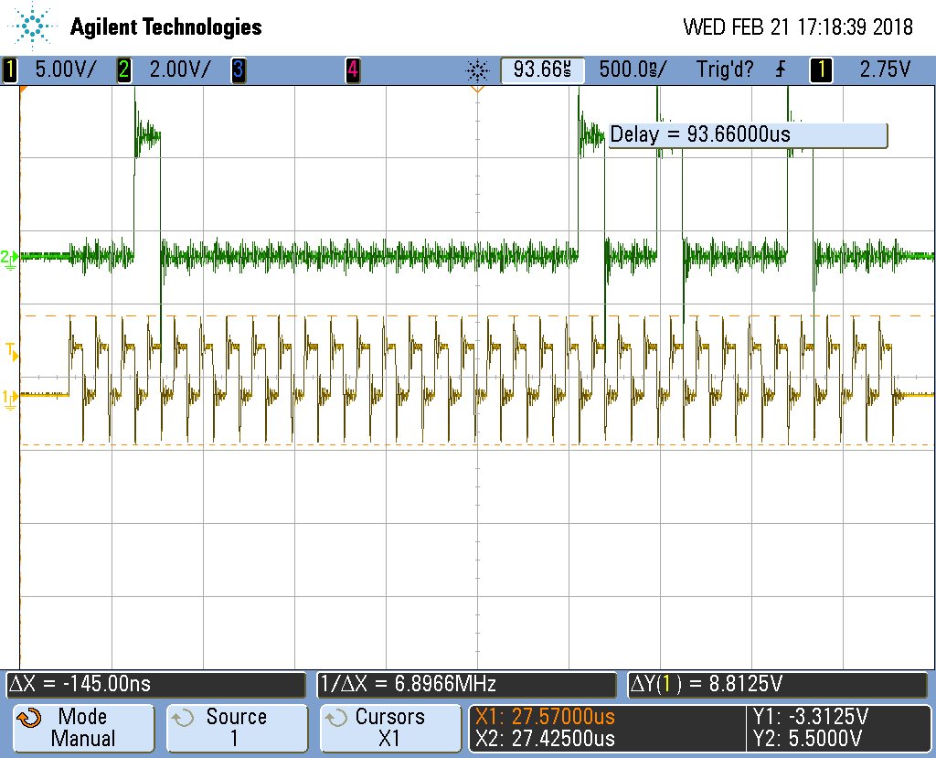
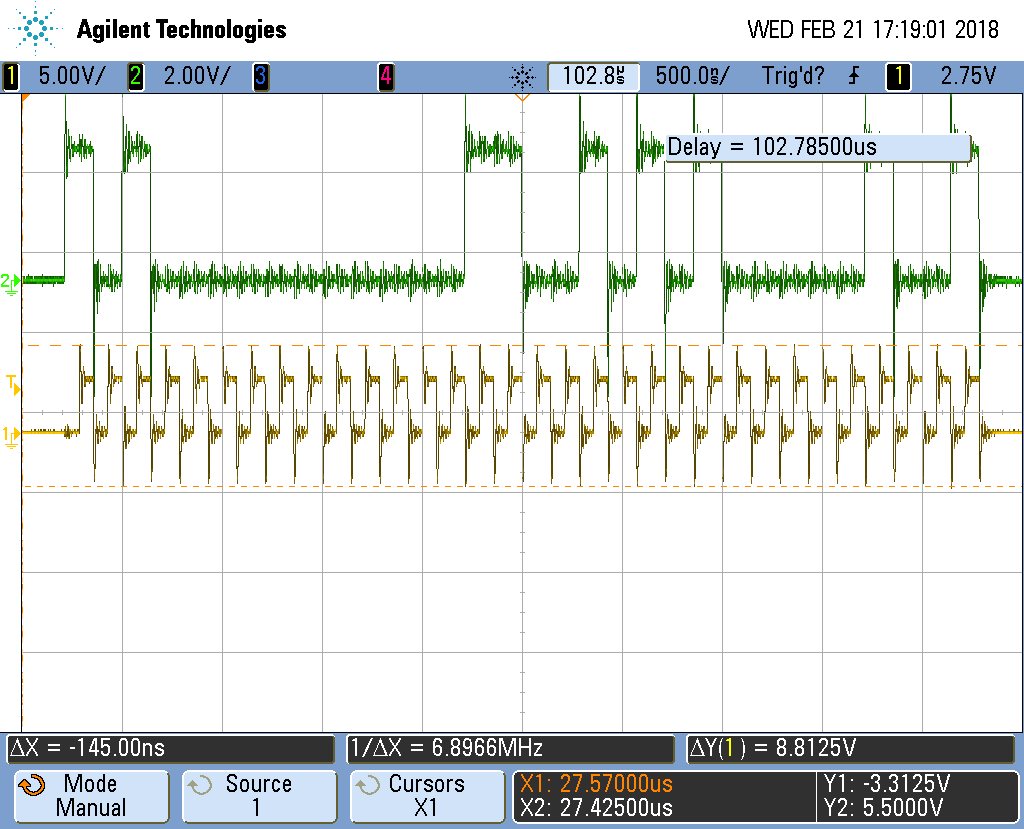
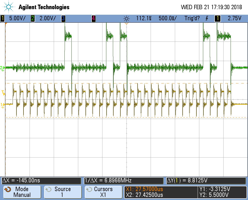
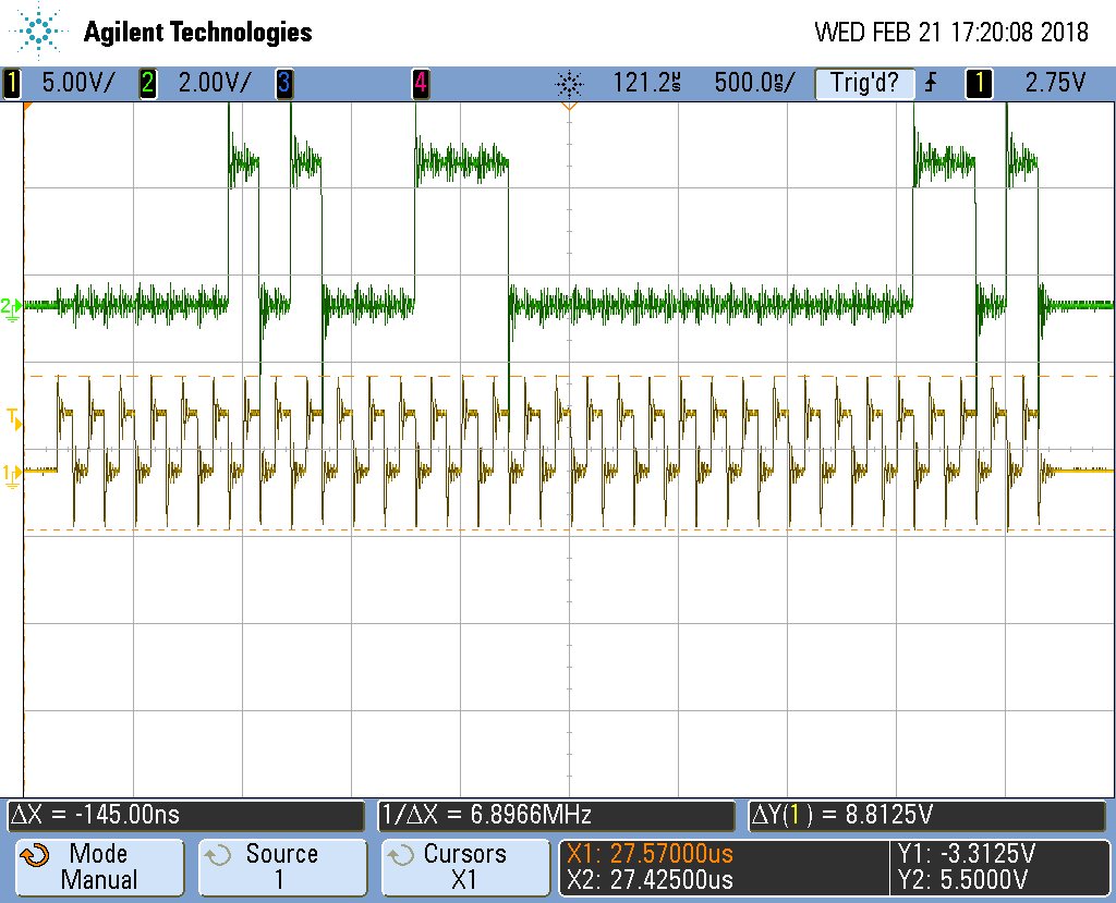
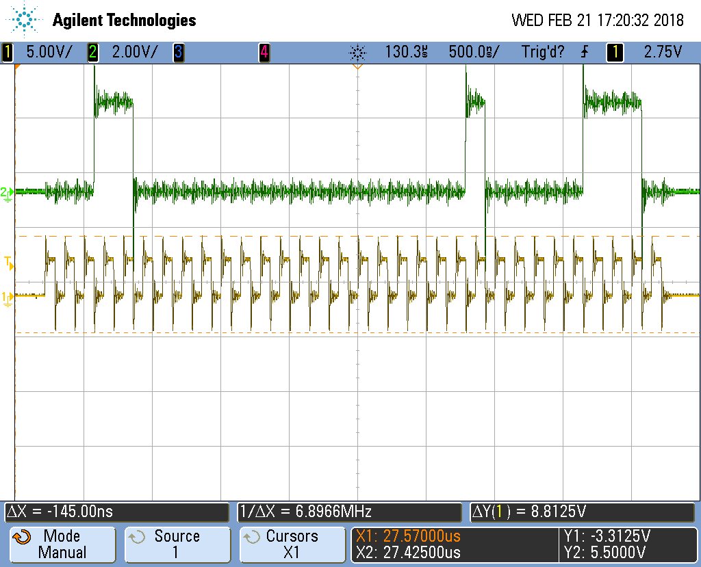
  • This is from an oscilloscope.

    The data is green, clock is yellow.

  • 32'h8000_0100,

    32'h8000_0100,

    32'h0000_0100,

    32'h0003_0301,

    32'h0000_0102,

    32'h0000_0103,

    32'h0000_0104,

    32'h0000_0105,

    32'h0000_0106,

    32'h0000_0107,

    32'h1000_0908,

    32'ha003_2a09,

    32'h0082_000B,

    32'h028E_00aD,

    32'h0803_020E,

    32'hCC00_180F

  • Dear Nikolay,

    thank you for sending the scope capture. You have LARGE amount of ringing here. Is this a scope probe setup issue ? I would try to reduce this ringing first. Add some series resistance on the line.

    Have you been able to verify your programming sequence against TiCS PRO?

    Regards, Simon.
  • Hello,

    I reviewed your programming, looks reasonable.

    This LMK03033 is on a board you designed or EVM?  How many boards are failing to lock?

    To debug the PLL not appearing to lock.  Please program the PLL_MUX = R Divider / 2 (should be write 0x18b0 020e).  Confirm that you see 14 MHz the LD pin.  If not what frequency?

    Next, please program the PLL_MUX = R Divider /2 (should be be write 0x1890 020e).  Confirm that you see 14 MHz at the LD pin.  If not what frequency?

    Finally, please advise the voltage of the CPout pin.

    73,
    Timothy

  • Timothy, Simon, thank you very much for your help!
    The problem was in our schematics. Namely, in the input stage of the circuit