This thread has been locked.

If you have a related question, please click the "Ask a related question" button in the top right corner. The newly created question will be automatically linked to this question.

CDCE62002: Fails to output a clock

Part Number: CDCE62002


Hi,

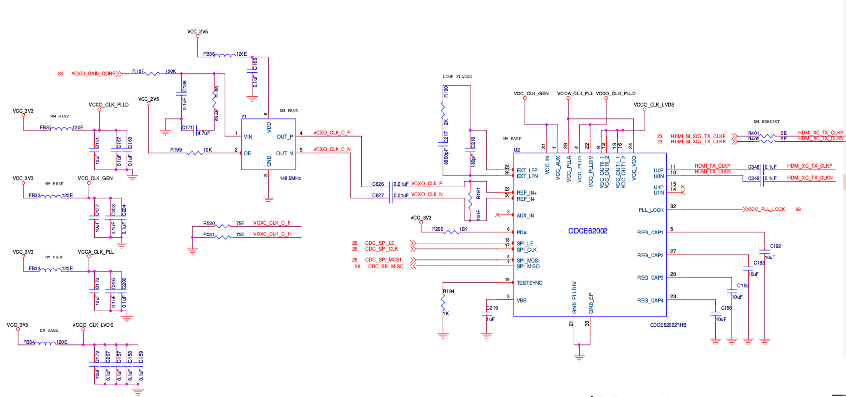
We have a design with a 148.5MHz input clock, and I'm trying to get the CDCE62002 to generate a 100MHz output clock - I will want different output clocks in future, but for now I'm trying to get 100M. I have tried all sorts of sequences of writing to registers, setting the PD bit to 1 before writing registers and then to 0 after writing registers, issuing PLLRESET etc.  Nothing seems to work - I don't get PLL_LOCK or a clock on the output of the device. Can someone summarise the required register sequence to get an output clock - I see conflicting sequences recommended by various people.

Thanks

Peter

  • Hello Peter,

    I assume you built a prototype board?

    Could you share the relevant schematic page?

    When you feel unconfortable posting in the forum, please refer to this thread and send it to .

    Can you please mention some of the frequencies you intend to generate in the future? Can you please share the requirements you have to the output clock, so I can evaluate the PLL setup?

    What is the input source? Is this a clean clock source or a jittery reference to be cleaned?

    Thanks!

    Best regards,

    Patrick

  • Hi,

    I have replied by email - here is the same information for others in future! Yes, this is our own board.

    The schematic:

    Initially we are looking at generating 100MHz purely for ease of verification. Our application will require 297MHz and possibly others. Based on these values, I have tried the following register values and written them to EEPROM:

    Reg0 =0x1037C240

    Reg1 = 0xFFB9AC41

    After power-cycling, I can verify that those values are there, but I don't have a clock on the output or LOCK.

    Let me know if you have any suggestions!

    Peter

  • Hello Peter,
    thanks for the schematic, this is very helpful to get a complete picture.
    Could you please test using 0x10B60240 and 0xBFB9AC41?
    I think you may have accidentally enterted a production test mode there by writing some reserved bits.
    Please let me know if the PLL locks now.

    Best regards,
    Patrick
  • Hi Patrick,

    Thanks for the suggestion: I have now tried the following:

    Reg0 =0x10B60240 as suggested

    Reg1 = 0xBFB9AC41 as suggested.

    Reg2 = 0x00000002 => power-down=0

    Reg2 = 0x00000802 => power-down=1 (i.e. power up the device again)

    This doesn't seem to work - is there something I am missing here?

    Thanks

    Peter

  • Hello Peter,
    let me try to reproduce this in our lab. As your EEPROM values come up properly, the load requirement seems to be satisfied and I do not see a reason why the device does not lock after your toggle !PD.

    Best regards,
    Patrick
  • Hi Patrick,

    I have managed to get the PLL to lock: the SPI interface was driven by a CPU at 10MHz, which should have been fine. I replaced it by a custom FSM in an FPGA, and now the PLL locks.  So, there was something wrong with the way the CPU was driving the SPI. We would like to understand exactly what was wrong with it, but don't have time right now - we'll get back to it at some point. For now, we have a solution which appears to work.

    Thanks for your help

    Peter