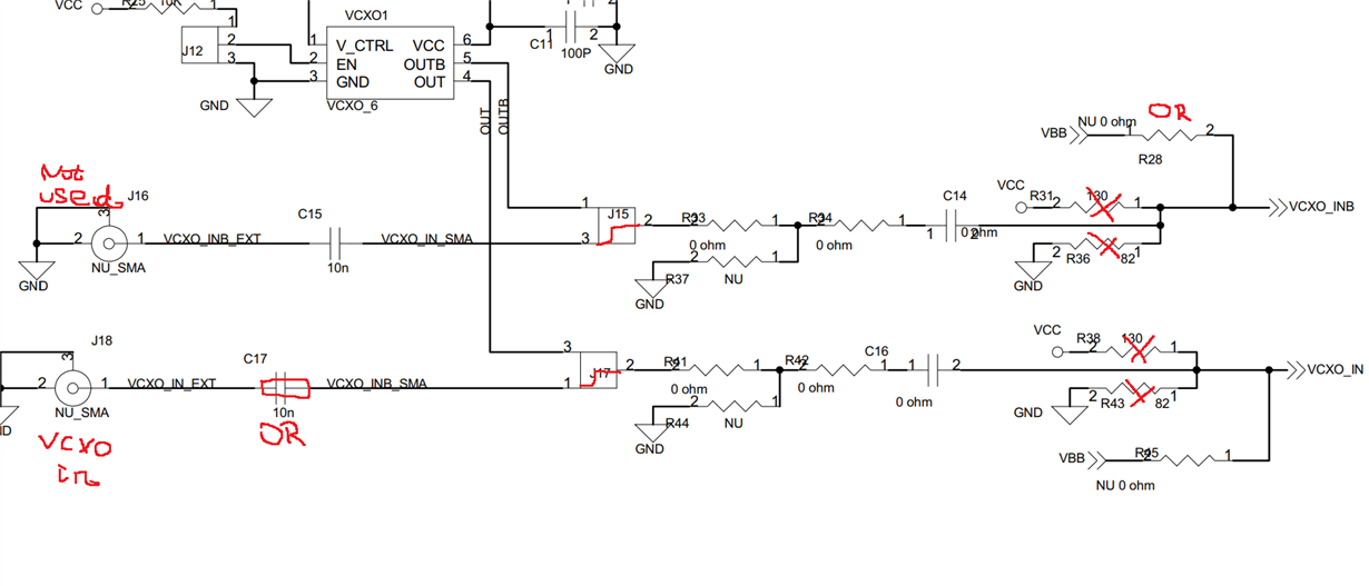
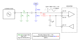
We want to use CDCM7005 to improve clock jitter. The evaluation board (CDCM7005-SP Evaluation Module) is configured to work with PECL VCOs although we plan to use LVCMOS 100 MHz VCXO. The board is populated with PECL terminating resistors (130R to Vcc and 82R to GND) for both VCXO_IN and VCXO_IN_N inputs and there is a pin providing VBB to bias unused complementary input.
My question is: what is the proper way of interfacing LVCMOS VCXOs to CDCM7005?
I plan to:
- remove terminating resistors from PCB at VCXO_IN_N input (R31, R36). Connect input to VBB bias volatege via jumper (R28).
- remove terminating resistors from PCB at VCXO_IN input (R38, R43), remove AC-coupling (C17 - jumer 0R).
Please share your comments.
Kind regards,
F.


