This thread has been locked.

If you have a related question, please click the "Ask a related question" button in the top right corner. The newly created question will be automatically linked to this question.

CDCLVC1310: Bypass mode for the Crystal-oscillator input

Part Number: CDCLVC1310

Hi team,

I have a question about the bypass mode for the crystal-oscillator input.

If I set the input clock select pin to 11, it means I choose the XTAL bypass mode.

So it means I can connect a 50MHz crystal-oscillator directly to the XIN pin and XOUT pin without the C1, C2 and R. Is it correct?

Another question, when is recommended to select the bypass mode?

Thanks a lot!

Lacey

  • Hi Lacey,

    Yes, your understanding is correct. It is recommended to use bypass mode if the crystal input is not used as the internal oscillator stage will be bypassed and improves power consumption.

    Kind regards,
    Lane
  • Hello Lacey,
    I'm going to confirm with our expert on this.

    Best regards,
    Patrick
  • Hi Lane,

    Thanks for your reply!

    So for the bypass mode, I had better choose a high performance crystal oscillator? Is it correct? 

    In addition, could you help to introduce the difference between the XTAL mode and XTAL bypass mode? Like the difference of internal circuit of our part and the performance difference?

    One more question for the output current.

    I just find in the datasheet for the output current is in the RECOMMENDED OPERATING CONDITIONS

    So are the IoH and IoL the maximal total output current? It means for the 10 output, the maximal current of each output is 2.4mA?

    Thanks a lot!

    Lacey

  • Hello Lacey,

    for a crystal oscillator you can omit the external load cap.

    The integrated load capacitance for the crystal stays in place for both operation modes of the XIN input.

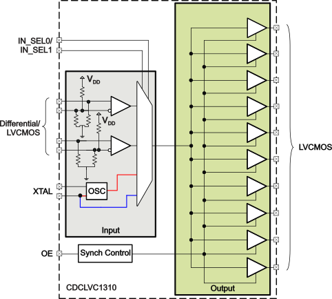
    Depending on the drive capability of your crystal oscillator it may be required to reduce the swing for the IN_SEL[1:0] = 0b10 mode, as the maximum swing shall not exceed 2 V. As there is some bias circuitry for the crystal, you will need the AC-capacitance to avoid impact on the crystal oscillator output stage.

    In the "bypass mode" a separate input buffer is activated which bypasses a portion of the crystal oscillator and deactivates the bias circuit. Therefore it is possible to provide a normal LVCMOS signal up to full swing of VDD.

    Input Selection
    IN_SEL1 IN_SEL0 Input Chosen LVCMOS Max Swing
    0 0 PRI_IN
    0 1 SEC_IN
    1 0 XIN, Crystal Input Stage 2 V
    1 1 XIN, Crystal Input Stage, Bypass Path VDD

    About the currents: 24 mA is per LVCMOS output. You have to consider in application that this limit cannot be exceeded when a short would happen.

    Best regards,

    Patrick