This thread has been locked.

If you have a related question, please click the "Ask a related question" button in the top right corner. The newly created question will be automatically linked to this question.

CDC3RL02: The specification of Master clock input (MCLK_IN)

Part Number: CDC3RL02


Hi,

I designed my clock circuit using CDC3RL02, I have a question about MCLK_IN of this buffer.

Does the buffer accept an AC-coupled clock signal as input for MCLK_IN? (The input signal into MCLK_IN in my design is as AC-coupled sinusoid signal from OCXO) 

It is specified the specification of MCLK_IN on page 6 the datasheet as below. I think this means that input signal into MCLK_IN should be DC-biased signal. 

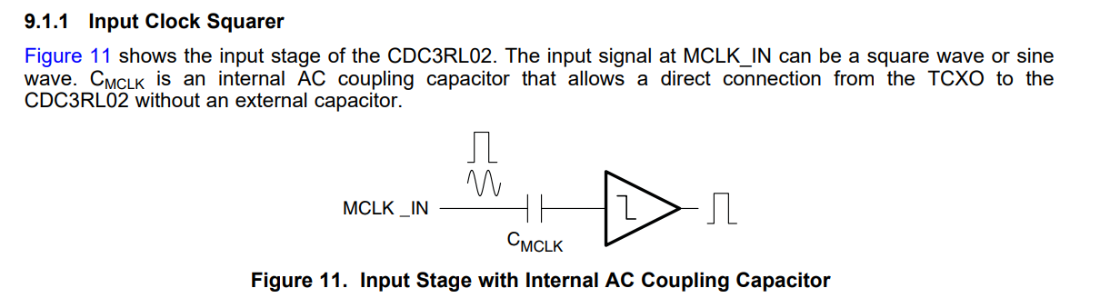
But, on page 11 of the datasheet, there is an AC-coupling capacitor inside the MCLK_IN input as below. I think this means that an AC-coupled signal is also acceptable. So, I am confused. Is it possible to be applied AC-coupled sinusoidal clock into MCLK_IN?

I would appreciate your advice.

Thanks.

  • You can apply an AC-coupled signal to MCLK_IN. The AC-coupling capacitor is included on the MCLK_IN pin as indicated in Figure 11, therefore CDC3RL02 will also accept a DC-coupled input.

    Kind regards,
    Lane
  • Hi Lane,

    Thank you for your answer.

    I have two more questions.

    1. The range of MLCK_IN on datasheet limits negative signal in Absolute Maximum Ratings to -0.3V and to Zero volt in Recommended Operating Conditions. On other hand it shows AC coupling inside, it means AC-coupled signal is acceptable as you said. These parts are contradictory. How is your thought?

    2. I actually tried applying an AC-Coupled signal to the input pin. When the Vp-p of the signal is about 500mV, the buffer generates duty-cycle distortion. What exactly is the voltage threshold of the input?

    Thanks  

  • Q1. The range of MLCK_IN on datasheet limits negative signal in Absolute Maximum Ratings to -0.3V and to Zero volt in Recommended Operating Conditions. On other hand it shows AC coupling inside, it means AC-coupled signal is acceptable as you said. These parts are contradictory. How is your thought?

    A1. Thank you for pointing out the MCLK_IN datasheet limits. The datasheet is incorrect. I will update the MCLK_IN limits in the next revision.

    Q2. I actually tried applying an AC-Coupled signal to the input pin. When the Vp-p of the signal is about 500mV, the buffer generates duty-cycle distortion. What exactly is the voltage threshold of the input?

    A2. What distortion are you measuring? For a 50% duty-cycle input, the output duty cycle will be 45% - 55% (see datasheet table 7.5).

    Kind regards,
    Lane