This thread has been locked.

If you have a related question, please click the "Ask a related question" button in the top right corner. The newly created question will be automatically linked to this question.

CDCLVP1208: clock problem

Part Number: CDCLVP1208


Dear sir:

   With using the CDCLVP1208 chip ,I have  a problem please help me.

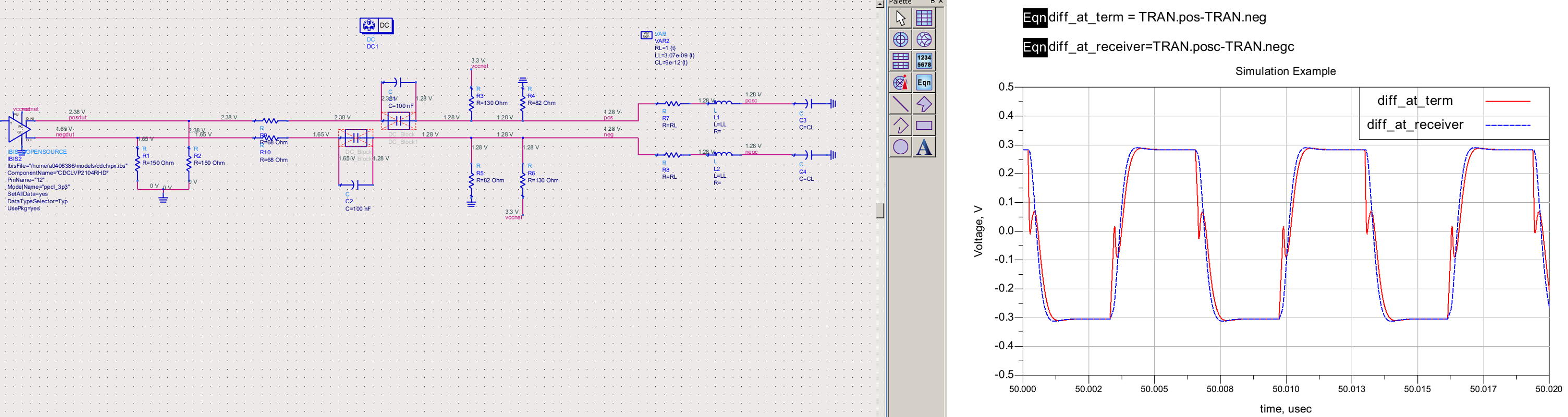
    When  I used the Tek oscillator to measure the 156.25M clock  at the end of the phy chip,(measuring with the difference probe ),I found the signal quality of the clock is not good and have a deep ditch at the edge of the rising and falling .

   So how can I eliminate the ditch and get a good waveform about the 156.25M clock.

   By the way ,the phy chip interface circuit is LVDS  and the CDCLVP1208 is LVPECL,so we use the  ac-coupled between the clock buffer and phy chip.At the end of the chip,terminal circuit is also be implemented and the pull-up resisteors is 130ohm and the pull-down resistors is 82 ohm .

Schematic file:

waveform file:

  • Hello user5049176,
    unfortunately your schematic and waveform upload were not successful. Can you please try one more time?
     
    Could it be that your receiver has an internal bias voltage generator and with the external termination this is shorting to different operating point?

    Thanks!

    Best regards,
    Patrick

  • Dear sir:

        Whether I have mount the bias resistor or not,the measured signal always have a deep ditch.The schematic and wavefile as attached file.

    waveform file :

    M09_CLK _ P37-CLK.pdf

  • Hello user5049176,

    thanks for sharing the info again!

    Typically this reflection is caused by the load from the receiver. Typically you can check this using the IBIS or SPICE model of the part. The receiver acts as non-ideal load next to the termination where you take the measurement. The length of the "stub" to the receiver load to the termination determine the reflection/glitch.

    Here a quick example how this could be caused. Using your actual receiver model and the IBIS model from our website, you should be able to verify that at the receiver the signal looks ok. (Iny my quick example I modeled the receiver as lumped model of package and receiver load. My values are somewhat pessimistic to make the effect more clear.

    Best regards,

    Patrick

  • Hi Patrick,

         The waveform was the same when measured at the pin of the reciver;

         If the "stub"contains the length from the pin of reciver to the die of it? Is there any way to verify your simulation by measuring waveform?Pls help to provide some ways to verify this issue,Thanks!

  • Hello user5049176,

    you can find the IBIS model for CDCLVP1208 here.

    Best regards,

    Patrick