This thread has been locked.

If you have a related question, please click the "Ask a related question" button in the top right corner. The newly created question will be automatically linked to this question.

LMX2492: Cannot change VCO Frequency or start ramping

Part Number: LMX2492
Other Parts Discussed in Thread: LMX2595

Dean,

I've been trying to get the LMX2492 to work, just to replicate the continuous sawtooth ramp in the EVM user guide.  I have trouble changing the VCO frequency, and can't see any ramping at all.  I cannot replicate any of the user guide examples.

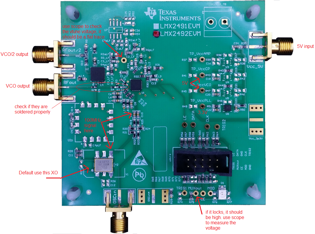
I can tell the board is alive, toggling the PowerUp/PowerDown register changes the current draw by maybe 20 mA.  Similarly, when I set the Mod, Trig1, and Trig2 pins to be input, I can watch them go high and low when I toggle the checkbox in the GUI, monitoring them with my multimeter.  On my Spectrum Analyzer, when there is 5V going to the the EVM, in Power Up mode, I see a CW signal a 4.46 GHz out of the RF/2 port.  In Power Down mode, I see 4.51 GHz.  Changing the VCO GUI field makes no change on the output.  

I'm hopeful maybe I have a setting wrong.  Or maybe there is a blown passive in the VCO chain, because it is suspicious that the CW sits right at 9GHz, when the EVM documentation says it should go from 9.4 to 10.8 Ghz.  When I put in Default Configuration from '2016 - 6 - 17', I have no improvement or change.  However, I'm holding onto the fact that I haven't had the 'Write Error' that I had when my LMX2595 board seemed to brick.  

What do you recommend?  Please and thank you for your help,

Darren

  • Darren,

    Sounds like you just want to start with a locked PLL, so lets go for that ...

    1. Establish communication -- Done
    The fact that you can send serial commands to power the device up and down and toggle I/O pins establishes that you are able to send commands to the device and the device is able to understand them.

    2. Load default mode
    We're in the debug process, no need to add any additional factors until you can get the PLL to lock.

    3. Check Input Frequency -- I think this could be the issue
    Ensure that you have 100 MHz input frequency. Yes, there is an XO on the board, but it is NOT powered up or hooked up by default. Ensure you see the 100 MHz input at the pin. So start with a 100 MHz input to the OSCin input SMA and verify that it is making it to the pin on our device.

    4. Check VCO Output
    Realize that the LMX2492 does not create an output, but only steers the VCO output. I don't know the exact range of the VCO, but it is wider than 9.4 to 10.8 GHz, as they have to have some margin. There is also a divide by 2 output. So if you see 4.46 GHz at the divide by 2 output, this means 8.92 GHz at the VCO, which sounds like the VCO is producing its lowest output frequency. I would check the VCO tuning voltage and I bet it's 0V.

    5. Check VCO tuning voltage
    Now try to make the VCO frequency and tuning voltage move. Try toggling the phase detector polarity on the TICSPro GUI from "-" to "+". This typically makes the VCO tuning voltage to go to the maximum value and also I would expect the VCO frequency to move. If you don't see the tuning voltage move, something is suspicuous. Maybe the loop filter is disconnected, shorted to ground, charge pump is tri-stated, ect.

    6. Read back the N divider and R divider outputs.
    On the MUXout (or other I/O pins), you can see the PLL R divider and PLL N divider. On this pin you can see the output of the N and R dividers as the chip interpretes them to be. Ensure that this frequency is correct and that it is not too low (sensitivity problem) or too high (sensitivity or hamrmonic problem)


    Regards,
    Dean
  • Dean,

    Great to have your help!

    I did 2. For 3 I see power going to the XO chip, and I can measure Voltage on the output of the XO, so I think I'm ok there.
    For 4, ya, I was thinking something like that. I measure Vtune as .6V and it doesn't change even when I set the GUI VCO frequency at something different.
    5: Toggling the CPPol doesn't do anything, which I believe is what you meant. So now we're getting somewhere. How would I test those other possibilities you mention?
    6: I'm not sure how to interpret what I should see on these outputs. Whereas a flag has either a High or Low state, the dividers should have some sort of number. Am I looking for a count on the pin, that is, P number of pulses to indicate the R/2 is at value P? What would I be triggering on to see this. Or maybe more basically, what mode should the I/O pins be in for me to be able to "see the output" of the dividers?

    Thanks,
    Darren
  • Darren,

    I'm assuming you are using our TICSPro software, but it would be good to know.

    Here's some things:

    After setting default mode, cycle power, toggle SWRST bit, and push Ctrl+L to make sure that we start off in a known state.

    2: OK. As we are missing something, we can be absolutely sure of this with step 6. So lets go to the next one.

    6: For this one, we want to see what signal the part believes is at the OSCin pin. To do this, do the following:
    a. Set MUXout_MUX = "Output R/2" state 16
    b. Set MUXout_PIN = "Output PP" State 2

    The output is the frequency after the PLL R divider then divided by 2 again (divide by 2 makes a nice square wave); it's not a number of fixed pulses as you say above.

    Now look at the MUXout pin on the oscilloscope and you should see half of hte input frequency. So if the reference is 100 MHz, you should see a 50 MHz square wave. If you a higher multiple, it could be a haronic. If you see nothing or noise, it could be a sensitivity problem and this implies the signal is not getting to our pin. Realize also that if you have no signal going to this pin, it can self-oscillate, although it will be way off from the target freqeuncy. If you are absolutely sure that there is indeed a signal at the OSCin pin, yet the part says nothing is there, consider some ideas. First of all, signal should be AC coupled and bias level on OSCin pin should be Vcc/2. If it is some issue with the pin, try driving the other compliementary output pin and see if there is some issue with the pin.


    5: Now assuming that we are sure we have the reference and the device sees it, focus back to the charge pump. Try toggling the charge pump polarity and then try an output frequency of 100 MHz and 20000 MHz and see if this moves the VCO. If not, consider these possibilities:

    a. Loop filter is shorted to ground. If so, you should see impedance =0 and short on board. If you see current to the board increase when you change the charge pump current, this could be an indicator.
    b. Loop filter is disconnected from VCO. This would mean bad connection for resistors R3_LF or R4_LF on the board.
    c. Charge pump Pin is damaged or shorted to neighboring pin. Hard to prove this, but if it doesn't toggle, something is off.
    d. If you did anything fancy with the loop filter or used any kind of active filter, then this could be an issue.


    REgards,
    Dean
  • Dean,

    I've asked Jeston to set up another phone call, because I'm not getting anywhere.  Hopefully we can debug it over the phone.  

    Yes I'm using TICS Pro.  I loaded all the defaults like you instructed.

    I redid step 3 from your earlier post, and found there is no clock coming out of the XO on the EVM board.  Power is going in, but no clock.  I cannot tell why it isn't connected, on the schematic and the board itself it seems connected.  Ok, so I connected a 100 MHz clock into the OSCin SMA like you suggested.  Then I connected my scope to the MuxOut pin, set to R/2.  

    I KNOW I'm sending in a 100 MHz clock, but I can't see anything on the MuxOut R/2 pin.  I have tried it on the other I/O pins as well.  I also connected the pin to my Spectrum Analyzer and could not so the signal at 50 MHz.

    So somehow the board cannot see the 100 MHz signal properly.  Hopefully a phone call can clear this up.  
    Talk to you soon,
    Darren

  • Darren,

    If you cannot get the right frequency out of the R divider "Output R/2" from the MuxOut pin, then this would cause issues getting the right charge pump voltage. Although you are putting a signal to the OSCin pin, I don't trust it is getting into the part. If anything is blow, it sounds like the OSCin pin.

    To test the VCO path, try this:
    1. Toggle the VCO phase detector polarity, it should cause the VCO to jump frequencies. But some parts use the OSCin pin to clock in programming bits, so if it doesn't work, it doesn't fully convince me that it still cant be related to the OSCin pin.
    2. Set the charge pump to "Disabled" in the TICSPro GUI. This disables the charge pump. Then apply a voltage of say 1 V and see if you can move the VCO voltage this way.

    I think that the "write error" is a red herring. This error has nothing to do with the actual device, but rather something with TICSPro. TICSPro is basing this error in any way based on how the device responds.

    REgards,
    Dean
  • Dean,

    I ran your two tests and the first one did not accomplish anything.  The second one, I am able to change the VCO CW spike when I apply different voltages to VTune.  What does this indicate?

    Thanks,

    Darren

  • I also just checked after C9, so at the 2492 OSCin pin, and I very clearly see a 100 MHz signal. So when you say the OSCin pin might be blown, do you mean INSIDE the 2492?
  • Darren,

    Potentially, this is something to rule out, but the 20 mA difference in supply current for powerup/powerdown now make me suspect an issue with unpowered power pins or some issue with the 3.3V regulator (U6). Initially, we had separate supplies for this board (5 and 3.3V) for evaluation purposes, but for later versions we hooked up the regulator. It seems like you have not had sucess so far getting other functions like the R/2 output or getting the charge pump polarity to toggle.

    Lets break this down:

    Programming:
    - Yes, the device is reacting to serial commands, but not as expected.
    - I/O pins can be programmed High/Lo
    - Current changes by 20 mA when powered up or down. So yes, it responds, but this should be more like 60 mA

    Power Supplies:
    Powerup/Power down test only makes 20 mA difference, but should make 60 mA difference. Sounds suspicious like unconnected power supplies. The board has a 5V supply for the charge pump pin, but it also has a bunch of 3.3V pins. that are supposed to be supplied by regulator U6. Can you verify this is the case? Can you verify that:
    a. Vcc_3p3V SMA launch pad is at 3.3V (driven by regulator)
    b. TP_Vcc_VCO test point is at 5V (pretty sure it is)
    c. TP_ Vcc_CP is at 5V
    d. TP_VccPLL is at 3.3V

    OSCin Pin:
    - There is valid signal going into the pin.
    - Have not validated that the device is actually counting this correctly. Issues that would cause this to count incorrectly could be: sensitivity level, matching issue, PLL counting harmonic instead of intended signal, blown pin, unintended noise/signal on complimentary OSCinM pin, or unconnected power pins. Note that if you are driving this single-ended, the unused side needs to see an AC coupling cap and 50 ohm to ground.
    - If you can't get OSCinP to work, then maybe OSCinN will work.

    Charge Pump Output:
    - It seems that you can steer the VCO frequency by manually applying a voltage.
    - It sounds like you were not successful getting the VCO to jump frequencies while toggling the charge pump polarity bit.
    - When powered up, VCO/2 Frequency is 4.46 MHz. When powered down, it's 4.52 GHz. This is suspicious. This is a positive coefficient VCO and I don't think that there are any active devices in the loop filter. So it sounds like when you power this up, it is slamming the VCO to the lower end of it's tuning range.


    Regards,
    Dean
  • Dean

    Power Supplies:
    A) The power pin of the 3.3 SMA pad is not driven. But I think that's because R49 is unpopulated. The Test Point at VccPLL is at 3.3V
    B) This is at 4.92V
    C) This is at 4.92V
    D) This is at 3.3V
    Just for ducks, I also checked that voltage after R30 and R32 are in fact 3.3V, and they are.


    I don't have a 50 Ohm load on OSCinN because the pad isn't populated with an SMA. But at this point, I actually took off my Signal Generator and can see the 100 MHz coming from the XO at the C9. I could connect an SMA on the pad and try and drive OSinN, but how would I turn off OSCinP?

    I think your assessment of the VCO railing sounds right. And then when I applied 1V and 2V to the VTune, it jumped up by maybe 40s of MHz.

    I think all of your summary is correct. So what should I do next?
    Thanks,
    Darren
  • What should I do next? (I accidentally clicked "this resolved my issue" but it hasn't been yet resolved. Thanks, Darren
  • Dean,

    I just got in a new 2492 board, and all the functionality works fine. I don't know what is wrong with the original eval board. But I'm moving forward. Thanks for your help,
    Darren

  • Hi Darren,

    Did you ever get it locked? Please check below.

    When the board is powered up, the current is about 170mA.

    After programming, it should lock. Current will go up to 225mA. LED will lit (the quality of the LED is not good, it may not work. so check MUXout to ensure you see 3.3V). Output is 4.8GHz at RFout/2 port. Vtune is about 2.44V.

  • Noel/Darren,

    I'm going to close this thread.

    It seemed that the problem was the original board had a hardware issue, possibly with the OSCin pin.  Whatever it is, it seems that there is now a working board.

    Regards,

    Dean