Part Number: LMK04828
I have an LMK04828B and I am trying to get dynamic digital delay to work. At the moment nothing happens, but I think the documentation is a bit confused (and confusing), so hopefully my mistake is simple.
I'm referring to two separate reference manuals:
- SNAS605AR – MARCH 2013 – REVISED DECEMBER 2015
This covers the LMK04828 which is my part, but as the instructions don't seem to work, I hunted out the latest revision - SNAS703 – APRIL 2017
This covers the LMK04828-EP which may be subtly incompatible, in particular this manual documents registers DCLKoutX_DDLYd_CNTH and DCLKoutX_DDLYd_CNTL (0x102, 0x10A, ..., 0x132) which are not mentioned in SNAS605AR.
In my configuration I have my VCXO running at 500 MHz (in nested 0-delay dual loop mode, feedback on DCLKout8) and am looking at DCLKout10 relative to my input reference clock.
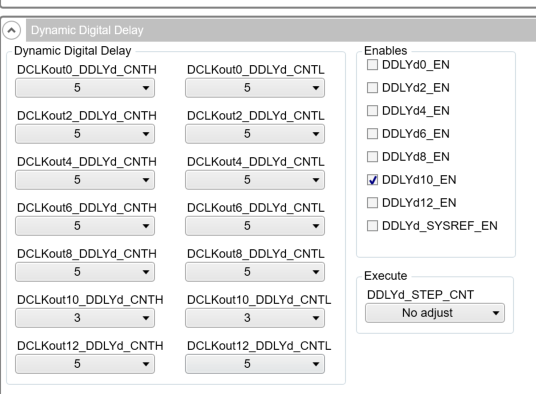
I have the following configuration for DCLKout10 (I don't think any of the other fields are relevant):
DCLKout10_DIV = 5
DCLKout10_MUX = 3
[0x12E] = 1 (only SDCLKout10_PD set)
After reset and full initialisation I then follow section 9.3.3.3 of SNAS605AR after setting SYNC_EN = 1 and [0x140] = 0 (so all SYSREF units powered on) and SYSREF_CLR = 0:
- DCLKout10_DDLY_CNTH = 3
- DCLKout10_DDLY_CNTL = 3
- (DDLY_PD already clear)
- DDLYd10_EN = 1 (all other enables clear)
- SYNC_DIS10 (so now [0x1ff] = 0xdf)
- SYNC_MODE = 3 (I gather that the assignment of 2 to this register in the following step is a documentation error)
- SYSREF_MUX = 2
- DDLYd_STEP_CNT = 1
Nothing happens, the phase of DCLKout10 remains unchanged. What am I missing?