This thread has been locked.

If you have a related question, please click the "Ask a related question" button in the top right corner. The newly created question will be automatically linked to this question.

CDCUN1208LP: Power sequencing issue

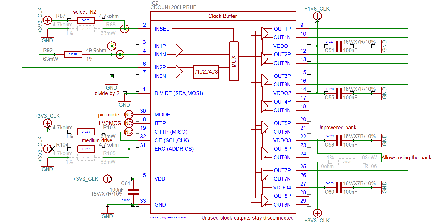
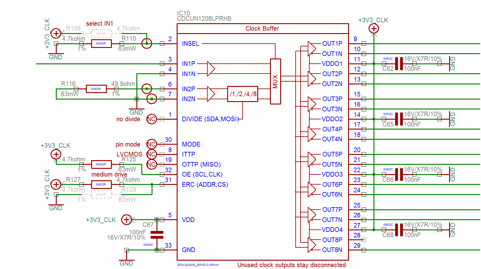
Part Number: CDCUN1208LP

I have an issue with the CDCUN1208LP when trying to power up. The configuration is as follows:

  • 3.3V powers the core (pin5) and VDDO4 (pin27)
  • 1.8V powers VDDO1 (pin11) and VDDO2 (pin14)
  • VDDO3 (pin22) is floating with a 100nF cap to GND

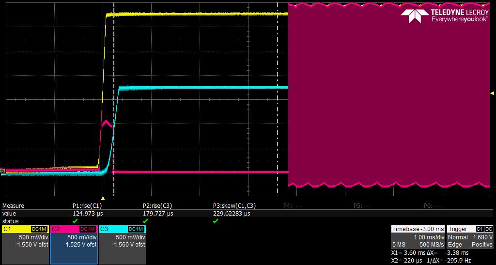
With the following sequence the CDCUN1208LP starts up and seems to work correctly - note the bump in the 3.3V before actual turn on.

CDCUN1208LP is working

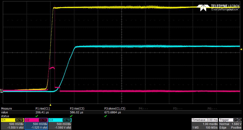
I cleared this bump (no other changes are made to the board) and with the following (nicer looking) sequence the CDCUN1208LP does not start anymore!

CDCUN1208 is not working here.

I think I respect all the power up requirements of the chip, i.e. >6.5V/ms rise time and core (3.3V) before or at the same time as VDDOx voltages (3.3V and 1.8V)

  • Dear Chris,

    I have assigned your question to an engineer.

    thank you for your patience.

    Regards, Simon.
  • Thanks a lot.

    Further, it may help that there are 2 more CDCUN1208LP on the same board seeing the same 3.3V core voltage (and ramp-up), however, these buffers' VDDOx are also connected to the 3.3V core voltage and these start in all cases correctly.

    Best regards, Christoph

  • Dear Christoph,
    I think this relates to the control pins and the 3.3V on the core voltage. The device samples some of the control pins only after internal POR circuit triggers to decide which mode it is running in. Pins like OE are continuously evaluated.
    I think in the earlier case with the bump, there was more delay between the 3.3V on the core voltage with respect to the 1.8V on VDDO.
    Let me check the details where the POR triggers and the sampling of the control pins happens.

    Best regards,
    Patrick
  • Here is the part of the schematic for this part, which may help you in your analysis:

    Clock buffer circuit

    I suspect somehow the input selection is not sampled correctly, although I thought it is (as the OE pin) always sampled.

    As I described previously, we use these buffers with a very similar configuration (see below) and they always start-up correctly in the 2 cases described in the first thread:

    Clock circuit #2

  • Dear Christoph,
    I can confirm that the internal logic is only connected to VDD, Pin 5. That means as long as your 3.3V power up clean, this should be working. As I can not explain right now why that is, I started to rework some boards in our lab to create your working and non-working configuration to reproduce the issue.
    Can you please let me know what frequencies you try to buffer?

    Thanks!

    Best regards,
    Patrick
  • Hello,

    We are buffering a 50MHz clock signal and as you can see in the pictures, we divide it to 25MHz with 3.3V and 1.8V outputs with one buffer (this is the buffer which makes problems) and we simply buffer the 50MHz with 3.3V outputs with another buffer (which does not make problems).
  • Dear Christoph,
    I could not replicate the issue you are seeing yet. I scheduled a power supply for tomorrow which can adjust the slew rate, so I can test it under similar condition.
    Did you try to do a "follow the fail swap" of the units?

    Best regards,
    Patrick
  • Dear Christoph,

    I tried your configs on a randomly selected EVM. Did you have a chance to swap the unit?

    Best regards,

    Patrick

    CDUN1208LP_e2e_supplyramps.pdf

  • Hello,

    The solution with the messier looking waveforms is working on 4 different sample boards we produced. I have not tested if they all fail with the nicer looking waveforms. I can try and repeat that measurement on a different board.

    But would you agree, that in principle the chip should start-up correctly with the waveforms as shown in the first oscilloscope picture? 

    Best regards,

    Christoph

  • Hello Christoph,

    please keep me updated, when there are specific units failing still when brought into a former working location, I would like to provide this to failure analysis lab.

    Please consider contacting me through the following mailing list or through your TI quality contact!

    Best regards,

    Patrick

  • Hi Christoph,
    "For proper device operation, the core power supply voltage (pin 5) must be applied either before the application of any output power
    supply or simultaneously with the application of the output power supplies. The application of an output power supply prior to the
    application of the core power supply could result in improper device behavior."

    I supposed that to delay VDDO 1.8V can help your mixed supplies application.

    Regards,
    Shawn
  • Hello,

    So I was able to test with other units and tried out slightly different configurations for the gating of the power supply rails for the CDCUN1208LP. The configuration where M1 and M2 are connected to the 1k resistor R1 and R5 works, whereas if I instead connect D1 and D2 to those resistors the buffer does not start up. In principle the resulting ramps look very similar (with slighly different slew rates, but all above the 6500V/s required).

    Power Gating Circuit 

    So here is the working configuration (with M1 and M2 pulling the gates low).

    CDCUN1208LP with M1 and M2 configuration

    Here is the not working configuration (with D1 and D2 pulling the gates low).

    CDCUN1208LP with D1 and D2 configuration

    In both cases the C2 trace (magenta) is one clock output supplied with 3.3V VDDOx. Due to the start-up of the oscillator (which is also supplied with the same 3.3V) the oscillation begins after approx. 4ms. The spurious signal during the ramp on the output of the clock buffer is appearing in both cases, which I did not fully expect, but could it be that the output buffers are in LVDS mode initially and then after correct reading of the ITTP pin switch to LVCMOS mode?

    However, I have working solution now (M1 and M2) with clean ramps. Although it would be good to understand exactly why the other configuration does not seem to work, I do not really have the means on our hardware to do extensive debugging and circuit modifications. I tested now 5 boards with this configuration and they all work under lab conditions.