


Part Number: LMX2581
Other Parts Discussed in Thread: LMX2541, CODELOADER, USB2ANY, PLLATINUMSIM-SW, LMX2531
Dear Sir,
Thanks a lot for earlier guidance for LMX2581 locking issues . It is showing lock on all frequency I made changes in my PCB Vbias VCo Cap chaged to 2.2 uF from 3.3 uF and VrerVCO cap changed to 1uF from 2.2 uF.
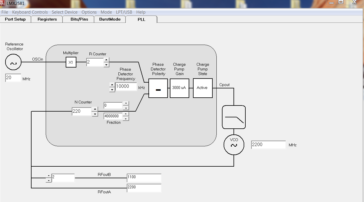
Now I am trying to optimize the phase Noise at 1100 MHz (using divide by 2 ) I set my Phase Detector frq= 10 MHz. I measured the Muxout (set for N/4 in code loader) in Spectrum Analyzer which should be 2.5 MHz which is very clean signal (very good Phase Noise) . The same I tried for Muxout (R/4) which is also very clean signal (very good Phase Noise) . The photos are attached by N_ref and R_ref.
But when I see the spectrum at 1100 MHz it phase Noise becomes bad at 10 KHz away from the Carrier. I set the Loop Bandwidth for 25 KHz and 48 deg Phase Margin Values for C1=1.8 nF, C2=56 nF, R2=390 Ohm, R3=270 Ohm, C3=3.3 nF as per evaluation board. But Nothing is improved. Can you suggest how can I improve my phase Noise (or How can I the spikes at 10 KHz way from the carrier) I I tried to changed the Phase detector Freq to 20 MHz but then also problem persists phase noise bad.The Spectrum attached as 1100_Spectrum
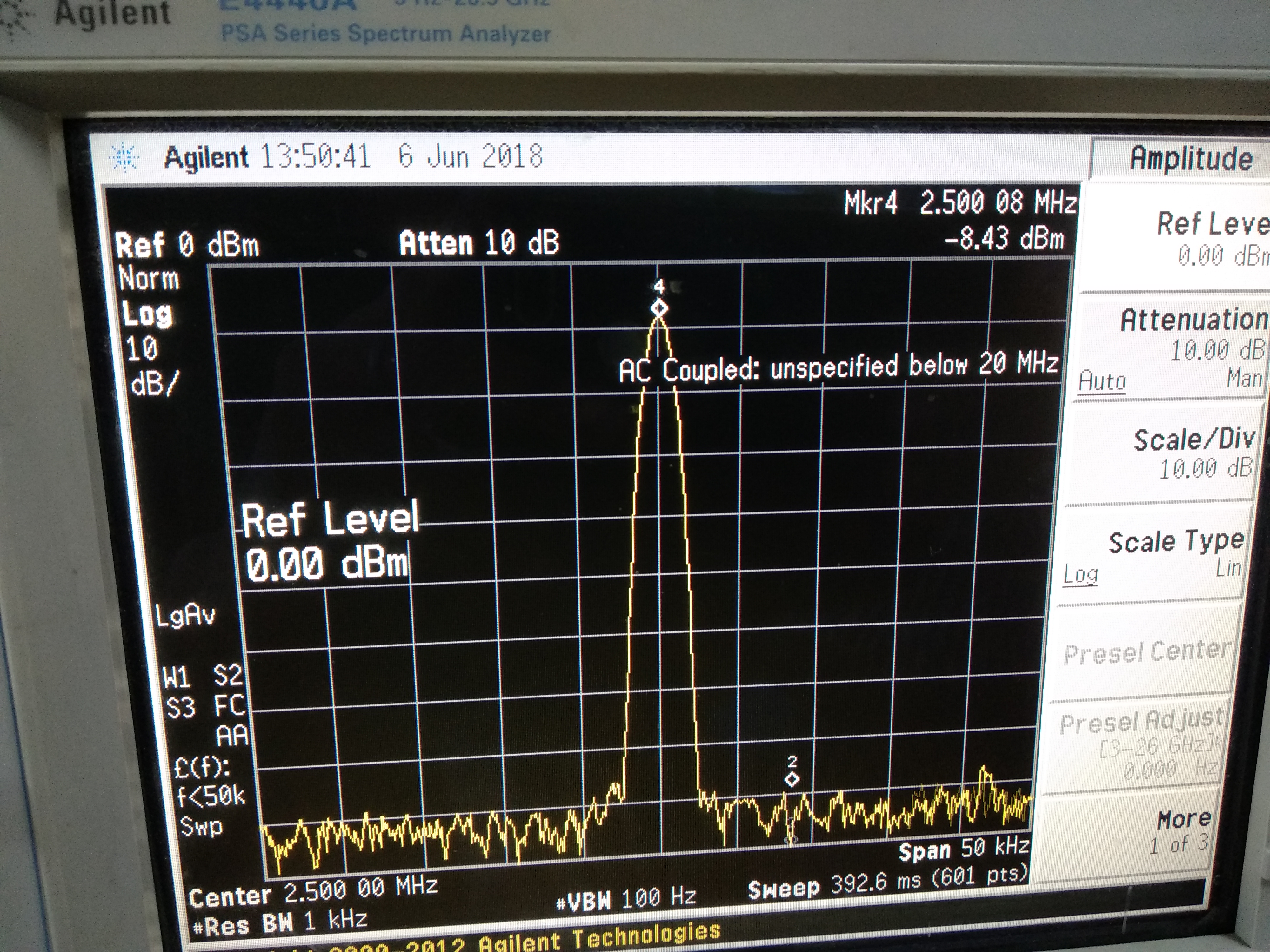
N_ref.PNG
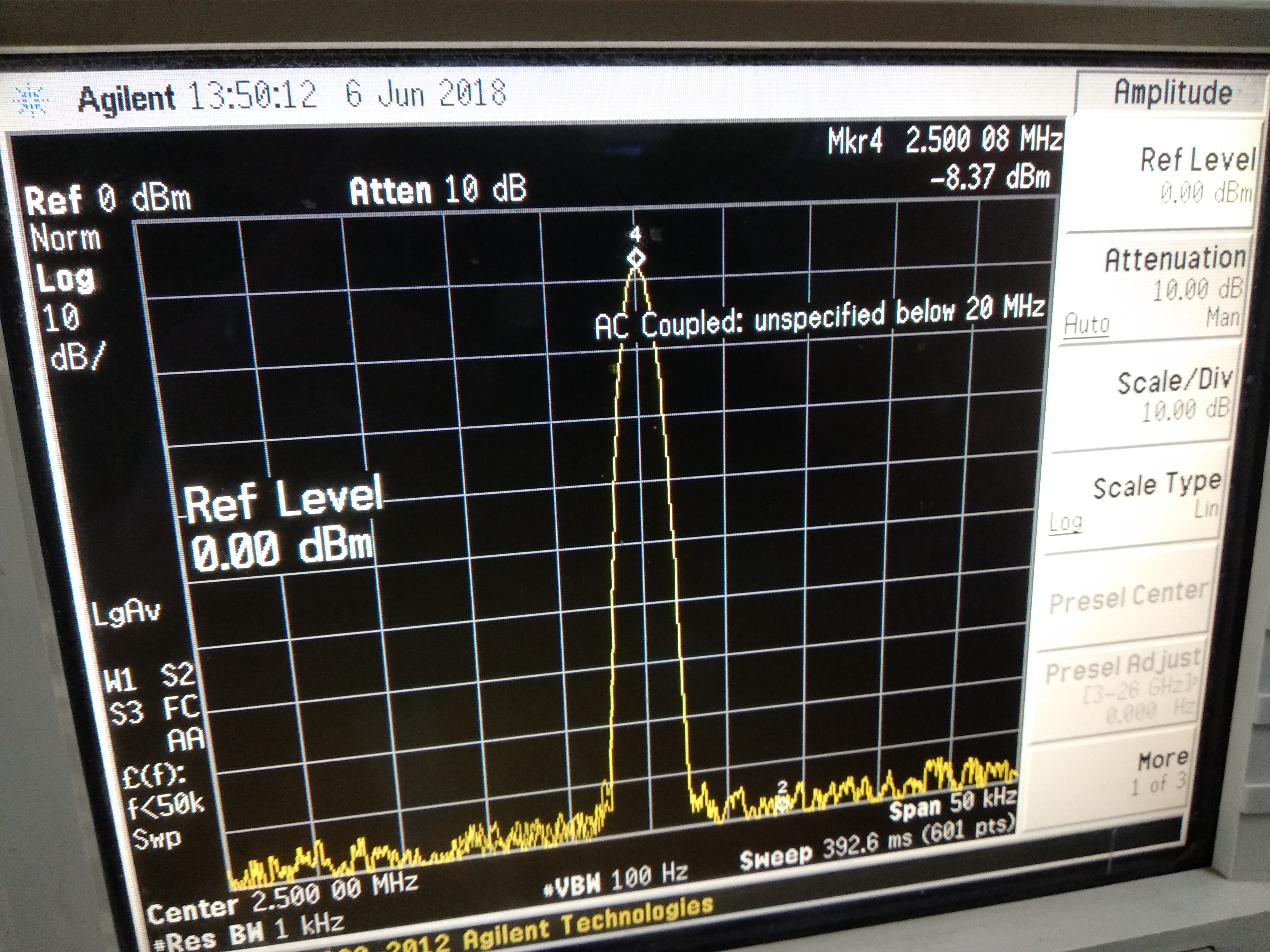
R_ref.PNG
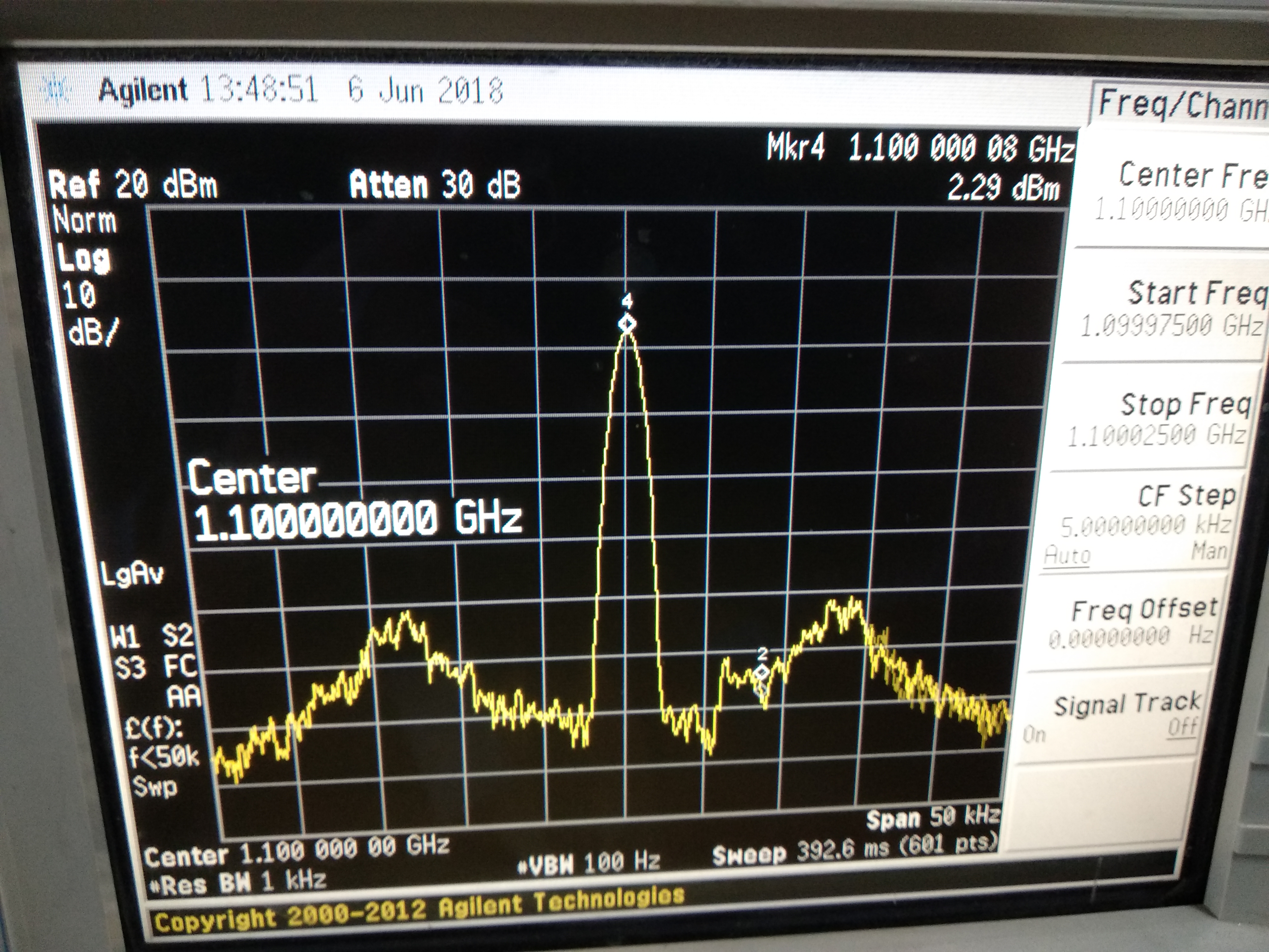
1100_spectrum.PNG

One more question which is related to environmental testing what should be the ideal loop bandwidth and phase margin for any LMX2581 or LMX2541 or other LMx PLL sothat it passes 6g rms vibration test.
Thanks in advance
Regards
LB Dube
Mirowave Systems

