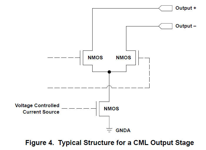
I find a strange description about the Vcm-DC of LVPECL/CML/LVDS from datasheet of CDCM6208:
LVPECL:
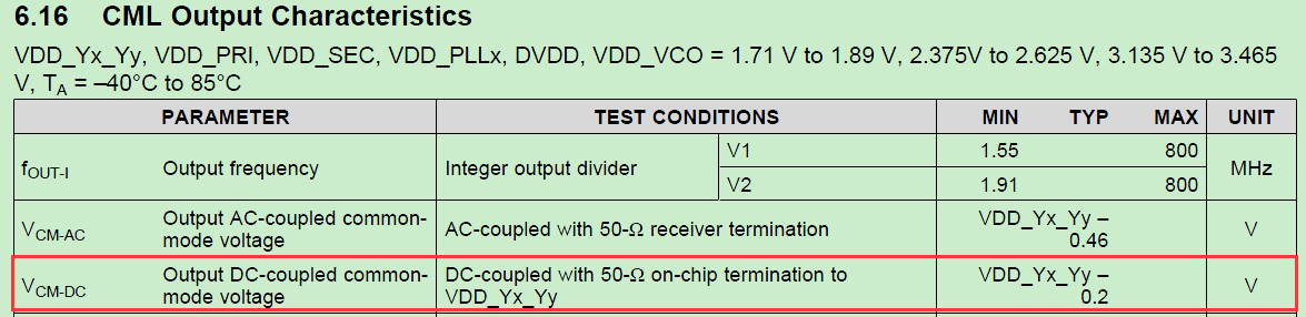
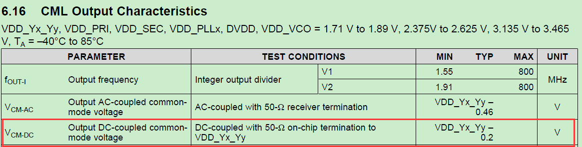
CML:
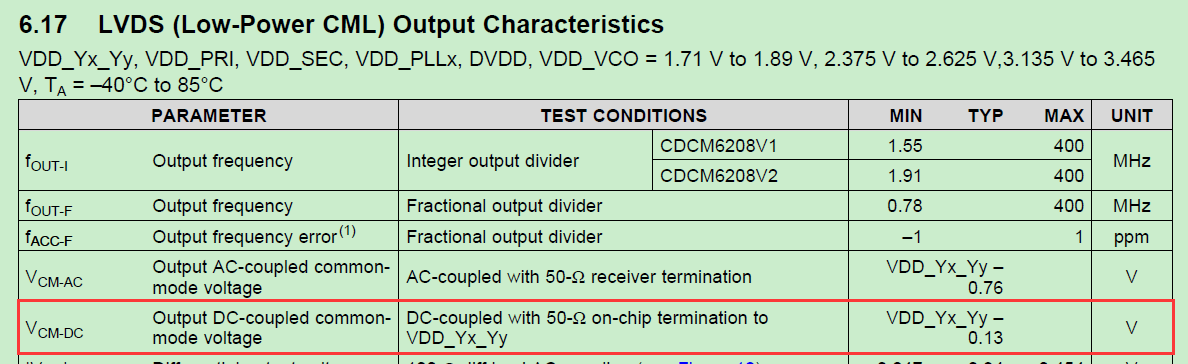
LVDS:
Can you tell me the actual model of DC couple? I want to know the test DC couple schemetic of CDCM6208's output,Thank you very much.
I find a strange description about the Vcm-DC of LVPECL/CML/LVDS from datasheet of CDCM6208:
LVPECL:
CML:
LVDS:
Can you tell me the actual model of DC couple? I want to know the test DC couple schemetic of CDCM6208's output,Thank you very much.