This thread has been locked.

If you have a related question, please click the "Ask a related question" button in the top right corner. The newly created question will be automatically linked to this question.

LMK00304: Input LVDS AC Coupling

Part Number: LMK00304

Hello Expert,

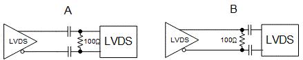
I have some question about input LVDS AC coupling configuration. It seems like there are two method. One(A) is placed termination resistor after capacitor and the other(B) is placed termination resistor before the capacitor. 

1. When customer should use type A and when they should use type B?

2. Is there any pros and cons between two configuration?

Best regards,

Alice

  • From the driver perspective, Type A is OK for LVDS drivers that can allow an AC coupled termination. DC coupled termination (Type B) is the standard LVDS termination and should be supported by all LVDS drivers.

    For LMK00304's LVDS driver, Type B is recommended because the DC coupled termination provides a DC current path to ensure proper output driver startup on power-up. If LMK00304's LVDS driver is configured for Type A (AC coupled termination), it is necessary to add a 1kohm bias resistor across the output pins (P & N) to provide a DC current path for proper driver startup.

    From the receiver perspective, both Type A and Type B assume the LVDS receiver has internal input biasing and no internal termination (since the termination is drawn as external).

    If the LVDS driver needs to be tri-stated/HiZ or held at a static output level (i.e. driver not toggling), then Type B is preferred if the LVDS receiver has built-in differential input offset voltage to avoid input chatter when the driver output is not toggling.

    LMK00304's differential input works well with Type B, since the input has weak internal biasing with -0.3V input offset voltage (VP-VN). If LMK00304's differential input is configured for Type A, the 100ohm input termination will override the internal -0.3V input offset voltage offset. In this case, we recommend to add a 3.3k pullup to 3.3V on the CLKin_N pin and 3.3k pulldown to GND on the CLKin_P pin; this will provide a small input offset voltage (~50mV) externally to avoid input chatter when the driver output is not toggling.

    Alan
  • Hi Alan,

    Thank you for the comment.

    By the way, why B is DC coupled termination? There are coupling capacitor between clock driver and receiver.

    Best regards,
    Alice
  • Hi Alice,

    The input impedance for a receiver is usually high. So, the termination is meant for the source driver. In type B, the termination is DC coupled to the LVDS driver.