


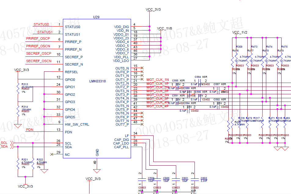
1.The clock output is for FPGA GTH port. It is LVDS signal. The required common mode voltage for FPGA input is 0.8V. How to configure the output clock?
Below is the schematic of customer, is it OK?
2.In addition, could the input frequency of primary reference and secondary reference be different? Such as, 25MHz Oscillator for primary and 100MHz Oscillator for secondary.
Thanks.
