This thread has been locked.

If you have a related question, please click the "Ask a related question" button in the top right corner. The newly created question will be automatically linked to this question.

CDCLVC1310: CDCLVC1310 - System-level additive jitter @30MHz and output load

Part Number: CDCLVC1310

Hi,

We are planning to use your Low Jitter clock buffer CDCLVC1310 to distribute our LVCMOS SiT5356 TCXO oscillator (datasheet link given below) output clock to multiple units by using coaxial cable.

www.sitime.com/.../SiT5356

In this our major requirement are given below,

No.of clock output : 7 (Min)
Output drive : 50 Ohm coaxial cable to another units
Phase noise degradation : Very minimum

Please find our LVCMOS oscillator phase noise at 30MHz output (which is input to clock buffer) for your reference.

1 Hz offset        -70 dBc/Hz
10 Hz offset      -98 dBc/Hz
100 Hz offset    -117 dBc/Hz
1 kHz offset      -138 dBc/Hz
10 kHz offset    -144 dBc/Hz
100 kHz offset  -144 dBc/Hz
1 MHz offset      -157 dBc/Hz
5 MHz offset      -158 dBc/Hz

Will it meet our above requirement or do you have any other better part for our application requirement?

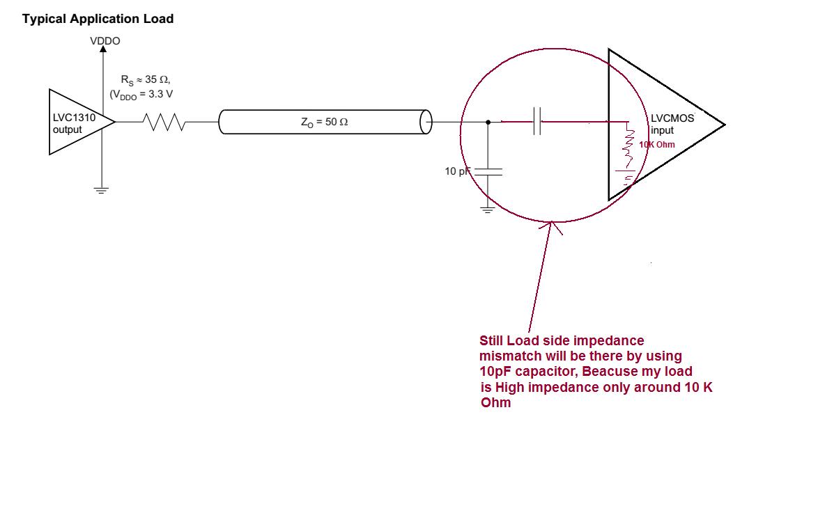
Also suggest if you have any application circuit for 50 Ohm load support.

Regards,

Sugumar K

  • Yes, CDCLVC1310 is a suitable choice.

    CDCLVC1310's LVCMOS outputs are intended to drive high-impedance LVCMOS inputs, so a 50-ohm termination is considered a heavy load. When a LVCMOS driver (with output impedance Ro) is driving a transmission line (Zo = 50 ohm), the line impedance matching is typically achieved using series termination resistor (Rs) closest to the driver, where Rs = Zo - Ro. See Figure 9 in the datasheet for typical values of Rs when Zo = 50 ohms.

    At the end of each 50-ohm coax cable, is there a 50-ohm load termination to ground? What clock signal levels do you require the load?

    Alan
  • Hi,

    We are going to use very small length co-axial cable (Approx 10cm) after buffer output and then we will AC-couple to our device at other end.

    We are planning to use some resistive termination before AC-coupling capacitor to avoid mismatch. Can we use 150 Ohms instead of 50-ohm which is too heavy load before AC-coupling capacitor?

    Also our load side we need LVCMOS/CMOS signal which can have maximum p-p amplitude of 1.8V?

    Also I have seen in your datasheet " Figure 2. LVCMOS Output DC Configuration; Test Load Circuit" the LVCMOS output is interfaced directly to 50 Ohm load.

    Can you clarify and suggest a application circuit for our application requirement?

    Sugumar K
  • I suggest using 1.8V VDDO supply for CDCLVC1310 and the following output interface circuit:
    Yx output (1.8V level) --- 20 ohms (Rs) --- [ 50 ohm coax cable ] --- AC cap --- Receiver device

    Rs provides series/source termination for impedance match, so there is no need for load termination (i.e. 50 ohm to ground).

    Alan
  •  Hi,

    I understood your solution will arrest only source side impedance mismatch not at load side. Please refer our typical circuit.

    Will it help adding 50Ohm series resistor with 500Ohms shunt resistor (potential divider) at load side instead of 10pF capacitor.

  • The series resistor (Rs) should provide source termination when the CDCLVC1310 LVCMOS output is driving a high-impedance load (e.g. LVCMOS input).  Rs should be sufficient for impedance matching the transmission line (50-ohm coax cable).

    Adding a 2nd termination at the load termination (Rt) may not needed and would form a double termination that would attenuate the driver's output voltage swing based on the voltage divide ratio of Rt / (Rs + Rt).  

    If your LVCMOS input buffer has 10k pulldown, you should not use an AC coupling cap since the 10k would pull the AC coupled signal toward ground.  If you use VDDO of 1.8V for CDCLVC1310, then you can DC-couple the clock signal directly to your 1.8V LVCMOS input buffer.  Otherwise, if you need to AC-couple the signal (e.g. to block DC between the driver/receiver), you may need to add an external bias network (e.g. 1k pullup to 1.8V, 1k pulldown to GND) to set the common mode voltage of the AC-coupled signal to the LVCMOS input.

    Also, you should not intentionally place a 10 pF shunt cap.  It was only included to model potential parasitic cap in a typical application load.

    Alan