This thread has been locked.

If you have a related question, please click the "Ask a related question" button in the top right corner. The newly created question will be automatically linked to this question.

LMX2594: LMX2594 Lock Issues

Part Number: LMX2594
Other Parts Discussed in Thread: LMX2592, TIDA-01410

TI E2E Clock Forum,


I previously had a productive dialog with Dean about our requirement to generate a 600MHz clock from a 1200MHz differential input source derived from a DDR4-based DIMM’s LVCMOS clock. We were successful when inputting our 1200MHz clock into the OSC inputs of the LMX2594 EVM demo platform. However, now we are attempting to generate the 600MHz clock on our hardware platform and are not seeing the same results. 

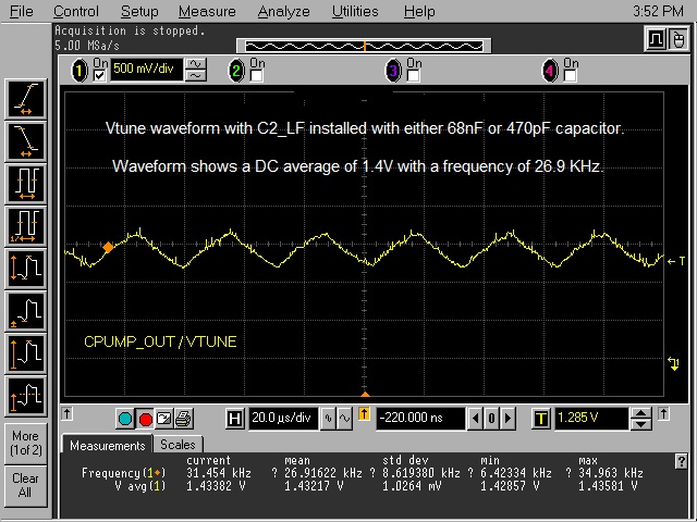
We have a very clean and monotonic 1200MHz differential input clock with ~ 2V P/P swing.  We are getting a very clean output clock from the LMX2594 with the 1.2V P/P swing we need delivered to the differential 100 ohm load at the destination FPGA input with the RF output strength set to 15.  Our 12GHz oscilloscope shows the output frequency to be very close to the 600MHz we require, but apparently not close enough as we cannot get the input and output clocks to sync on the scope shots as we did with the demo board bench setup in order to confirm deterministic phase lock.  I suspected that the loop filter might be the problem so I tried all the charge pump gain settings in TICsPro while monitoring the lock detect signal.  The only setting that gave us a constant lock indication was the 12mA setting.  The other settings resulted in either no lock or intermittent lock.  I realize that even a steady lock detect output is a ballpark  indication at best.  So we’re apparently close but not close enough.

Our hardware design is based on the reference design in the LMX2592 EVM User’s Manual.   We have been very liberal with bypass and bulk capacitors on the 3.3V rails and LDO outputs. The output circuit uses the 50 ohm scheme as recommended in the data sheet including the 18nH choke on the output driver power rail. The loop filter is similar to the TI design with the exception that due to space restrictions, we used 0201 components rather than the 0603 parts indicated in the BOM. The discretes in the loop filter are closely grouped on the pin 35 side of the LMX2594 with C4_LF placed as close to pin 35 as possible per the datasheet layout recommendations.   This is different than the demo board which has the loop filter discretes grouped on the pin 12 side of the LMX2594 on the demo board. I hope this is not a deal-breaker. We are using a 16-layer PCB with all the loop filter interconnects except the pin 12 connection on layer 1 with a full ground plane on layer 2. The pin 12 connection to the loop filter connects to the filter discretes using vias between layer 1 and layer 3. The OSC inputs are terminated with a 100 ohm resistor followed by two 0.1 uF AC coupling capacitors as in the reference design. We are using the EVM control module and TICsPro with the 10-pin connector to program the LMX2594. The following lines in the 10-pin interface are used: SDI, SCK, CSB, MuxOut, GND. The remaining pins are NO_CONNECT.

When we get our “lock” indication, the LMX2594 is programmed as follows:

Freq = 1200 MHz, Doubler = X1, PreR = 24, R = 1, Fpd = 50 MHz, Charge Pump Gain = 12mA, Included Divide = 4, N Divider = 48, Channel Divider = 16, RFoutA = 600MHz and VCO = 9600 MHz. VCO_PHASE_SYNC box is checked.

Your feedback and guidance in helping us debug this circuit will be most appreciated. I also noticed that there is a 10 August 2018 update on TICsPro which I hope to download and try tomorrow.

Thanks,

Ken

  • Ken,
    Sorry to hear that you are having issues.

    In general, the PLL output frequency should be exact, and if it is not, it sounds like some kind of issue. I don't think that using 0201 vs 0603 components would make a huge difference. The only clue I see is that it sounds like the design works better for 12 mA charge pump current.

    The original loop filter was designed for 15 mA charge pump current and 200 MHz phase detector frequency. If you keep the same loop filter components, but reduce the phase detector frequency to 50 MHz, then you will get a lower loop bandwidth. If you wanted the same loop bandwidth, then theoretically, the loop filter capacitors should be 1/4 of their original value and the loop filter resistors be 4x their value.

    I think that the loop filter is still stable (or at least theoreically it can be), but if you have two PLLs running simultaneously, then perhaps there is some sort of frequency pulling gong on. If you increase the charge pump current, it increases the loop bandwidth and helps the PLL fight the frequency pulling. Just a theory.

    Regards,
    Dean
  • Dean,

    Thanks for the quick reply.

    There is a JEDEC-standard RCD component near the LMX2594 which has multiple internal PLLs needed to generate 3 copies of the DDR4 input clock at 1.2GHz, one of which is the input clock to the LMX2594 OSC pins. In our layout, the CPOUT net is the longest routed signal that's part of the loop filter. If CPOUT is being victimized by crosstalk from one of those PLLs, would that possibly be responsible for inducing noise into the loop filter and causing the frequency pulling effect? If so, I could cut some traces and re-route the CPOUT signal to test this theory. Are there any other external signals I can probe that might shed some light on the issue?

    By the way, I loaded the Aug 10th version of TICs Pro and was gratified to see that the software now considers our configuration to be in Category 2 rather than Category 3.

    - Ken
  • Ken,

    Frequency pulling is sort of a tricky issue to deal with. Suppose that you have two LMX2594 devices and there is a frequency pulling issue. Here's some things that might impact it.
    1. If you increase the loop bandwidth (quick way is increase charge pump current or phase detector frequency), then it should be able to fight the frequency pulling better.
    2. Maybe if you can isolate the supplies to the pull-up, it could help.
    3. If you observe the spectrum of one to be noisy and then it cleans up when you power down the other PLL, it points to frequency pulling.

    The fact that our EVM doesn't show this and your does is what makes me wonder if it is something board related.

    Regards,
    Dean
  • Dean,

    We moved the unit under test onto a new platform which gave me slightly different results. Both OSC and Output traces still did not sync together, but we got a 99.9% duty cycle on the lock detect at 15mA. As we reduced the charge pump current, to 12mA ... 9mA ... etc., the lock detect duty cycle got proportionally worse. This seems to lend credence to your frequency pulling theory.

    Since TICsPro won't allow me to go above 50MHz on Fpd, I'd like to try your suggestion to change the loop filter discretes. If your suggestion is to increase the loop bandwith by a factor of 4 while keeping Fpd=50MHz, I don't understand changing both the Resistance to x4 AND Capacitance to 1/4. Doesn't this keep the RC time constants the same, which keeps the loop bandwidth the same? Wouldn't I want to keep the Caps the same and reduce the resistors by 1/4, for example? I'm probably wrong, but I thought I'd confirm with you before having the new values pulled from floor stock.

    Thanks,
    - Ken
  • Ken,
    So this seems like some sort of frequency pulling to me and wider loop bandwidths seem to help.

    In regards to the loop filter, if you increase the resistors by 4X and reduce the capacitors by 4X, then theoretically, all the time constants are the same.
    However the loop filter transfer function (2nd order) is of the form:

    Z(s) = (1/A0) * (1+s*T2)/(1+s*T1)
    Where A0 = C1 + C2

    So the action of reducing the capacitors increases the loop bandwidth and the action of changing the resistors is to try to preserve the same phase margin.

    Regards,
    Dean
  • Dean,
    Thanks for clarifying the discrete issue.
    In your previous response, Item #2, you suggested isolating the pullup power rail. Are you referring to the 50 ohm output pullup resistor? If so, I have already isolated the pullup rails to a point similar to the demo board. I'm using an 18 uH choke in series with the 3.3V rail with 2, 0.1uF bypass capacitors to ground. I noticed that the demo board uses a single 0.01uF cap after the choke. Would it help to change one of my 0.1uF caps to a 0.01uF cap? I also can add a 0402 resistor in series with the choke if you think that might improve the isolation.
    - Ken
  • Ken,

    Yes, I was talking about the 50 ohm pullup resistor. I'm not so sure that changing the capacitor will help that much. Theoretically, if you used an inductor instead of a resistor pull-up, that would help.

    You might want to look at reference design TIDA-01410, which is a dual LMX2594 PLL reference design.

    Regards,
    Dean
  • Dean,

    I have physically removed the IC with the 3 intrinsic PLLs to eliminate any possible frequency pulling contribution from them.  The result is a 100% lock detect duty cycle at 15mA charge pump current but still doesn't sync the input and output signals.

    I was wondering if another source of frequency pulling might be the high-current PWM input to a DC/DC converter inductor running somewhere between 500KHz and 1MHz?  The A channel LMX2594 output differential pair is routed near such an inductor pad.  If it's the frequency pulling effect, what would be the most vulnerable part of the LMX2594 circuit.  Would the output transmission line be a prime candidate?

    Thanks,

    - Ken


  • Ken,

    OK, so removing the other chips resolves the lock detect problem. Also, potentially you could power down just the outputs on an unused device and also see if this has an impact. As for your DC/DC converter, the pull-ups for the outputs is the most succeptible area. The LMX2594 has internal LDOs to protect the charge pump and VCO, so it is less succeptible. So yes, the output transmission line would be a prime candidate.

    As forthe device not syncing properly, I thought that this was working as it should be category 2 sync. It does require a software sync, but the timing of this is not critical. Also, note that the PLL_R_PRE divider has to be used due to the high reference input frequency.

    Regards
    Dean
  • Dean,
    Since my last reply, I have disabled all power supplies on the board including the on-board dc/dc converter that supplies 3.3V for the LMX2594 and brought in an external source of 3.3V from an HP bench supply. The LMX2594 input and output clocks still do not sync with or without VCO_PHASE_SYNC enabled and after the software SYNC is transmitted. However, we still have a solid lock detect at 15mA. I am using the same TICsPro settings as I used in my successful evaluation of the DEMO board using the same DDR4 differential input clock. The settings are as follows:

    Freq = 1200 MHz
    Doubler = X1
    PreR = 24
    R = 1
    Fpd = 50 MHz
    Charge Pump Gain = 15mA
    VCO = 9600 MHz
    RFoutA = 600MHz
    Channel Divider = 16
    SYNC input is set to IGNORE

    When VCO_PHASE_SYNC = 1: Included Divide = 4 with N Divider = 48

    I am not using the RAMP or SYS_REF functionality.

    The following items are where we currently deviate schematically from the EVM circuit:

    OSC differential input may have excursions slightly above 2V P-P.
    RampCLK, RampDir, SysRefReq and SYNC pins are currently floating, however, I have none of them checked in the Pins Section of User Controls in TICsPro.

    Can any of the above deviations contribute to the non-SYNC symptoms we are seeing? At a minimum, should I be connecting the 4 floating pins to a 12K pulldown as in the EVM design? Or is a direct connection to ground preferable?

    Tomorrow, I will review the EVM Gerbers to see if anything jumps out at me. If none of the above are causing the lack of SYNC, I guess the next thing to do is replace the chip, but since it is still generating a non-synced 600 MHz output clock, a bad chip is probably a long shot.

    Anything else I may have missed?

    Thanks,

    - Ken
  • LMX2594 Global Delay.docxKen,

    For what it's worth, I took my LMX2594 EVM and tested the lock detect in the setup condition you have and had no issues, even when I lowered the charge pump gain.

    The floating pins should not matter, but if you feel safter grounding them, or grounding them through a resistance, go ahead.

    I also tried the phase SYNC and was able to get a consistent phase relationship.  I was able to see this, power the chip up/down, ect. One thing that I did want to make clear that for the phase sync function, this simply produces repeatable delay.   However, there is no promise that this delay is zero or the same for every device.   The attached document discusses the delay varaition of the LMX2594.

    Regards,

    Dean

  • Dean,

    After further investigation, I determined that I had incorrectly reported the symptoms of our lock/sync failure of the LMX2594.  As a result of a BOM error, C2_LF was stuffed with a 470pF capacitor instead of a 68nF device per the EVM.  This incorrect device actually produced a 100% duty cycle on the lock detector but no SYNC between the input and output clocks.  When the error was discovered and we replaced C2_LF with the correct 68nF device, the lock detect duty cycle reduced to only 9%.  I should also mention that regardless of C2_LF value, the Vtune testpoint shows a triangle waveform at ~27KHz with a DC average of 1.4V.  This is in stark contrast with the absolutely flat response of Vtune at 1.26V that we observe on the EVM board when locked to the same DDR clock.  Does this imply that our lock failure is due to a loop filter problem after all?  Short of some unforeseen fabrication problem, I can’t suggest a mechanism for this obvious mis-tuning of the PLL.  A colleague has even suggested that the Intel platform generating the 1.2GHz input clock might be employing spread-spectrum at 5Kppm of the center frequency which might be throwing off the PLL.  However, this is the same clock we use with your EVM board which locks consistently.  

    Another wild card is that the 1800pF capacitor (C4_LF) is an X7R rather than a C0G/NP0.  Could this be a factor?

    Scope shots are attached.

    Thanks,

    - Ken

  • Ken,

    The action of probing the Vtune voltage could be loading this down, but if this is really what the Vtune voltage is doing, then I would not blame the lock detect for not being happy.

    If the period of the waveform lines up with phase detector period, then perhaps it is some kind of leakage or loading on the loop filter.

    I don't think that it's related to the VCO calibration, but a quick check is to set CAL_CLK_DIV=3 and see if this clears it up or not.  The fact that you are at 1.4 V sounds about right.  This voltage varies a little bit and also over temperature.

    Regards,

    Dean

  • Dean,
    I hooked up a 150MHz differential crystal oscillator on my unit under test similar to the EVM schematic in place of the 1.2GHz DDR4 differential clock. I adjusted the registers to generate a 600MHz output. It locked up and SYNCed as advertised. Lock detector has 100% duty cycle and Vtune is flat at around 1.3V. This is with loop filter components per the EVM schematic.

    Now I'm wondering if there's a problem with the 1.2GHz clock on the host platform. I'm now probing it directly on the LMX2594 inputs. The waveform seems to be a relatively jitter free sinusoid but it's about 2.7V peak-to-peak. The datasheet indicates a maximum input of 2.0V. Is there some wiggle room here, or is this an absolute maximum under any environmental circumstances? Would this explain the circuit's inability to lock/SYNC? Are there any other malicious input clock characteristics that would cause the lock to fail? We have verified that spread-spectrum clock modulation is disabled on this platform.

    Thanks,

    - Ken
  • Ken,

    Sorry to hear that you are having so much problems with this.
    There is nothing wrong with not connecting theses pins and overdriving the OSCin pin should not cause these issues, as long as both inputs have the same OSCin clock.

    Now when you say lack of SYNC, I'm not exactly sure what you mean. It's not clear if this means that the phase relationship between the two output devices is random (even after sync procedure is applied), or if you are expecting a phase relationship to be zero, when in fact it is not. If it is the later case, then just be aware that SYNC just sets up consistent phase between two devices, but not necessarily zero phase.

    Regards,
    Dean
  • Dean,
    The LMX2594 is now working correctly on our customer's platform. I appreciate your assistance in getting me up the learning curve and helping me navigate the process of elimination. In the end, it turned out that the input clock from our Intel DDR4 platform was operating either in bypass or spread spectrum mode in the early phases of boot up which appeared on the scope to be a solid 1.2GHz clock. However, it wasn't pure enough to satisfy the input requirements of either the EVM or our target implementation. Once we realized this, we made the appropriate adjustments in the platform BIOS and achieved a solid lock detect and a flat Vtune output at ~1.32V. The main takeaway from this is that the LMX2594 (using the EVM reference design) will not lock to a JEDEC-standard DDR4 clock while in spread-spectrum mode.
    Thanks again for all your help.

    - Ken