Dear,
I would like to ask a question regarding the CDCE62005 chip's operation.
I have used both TI GUI tool (CDCE62005 EVM Software 1.4.8) and my own calculation to yield the register table for configurating the chip. However, I failed to set my desired frequency at the outputs.
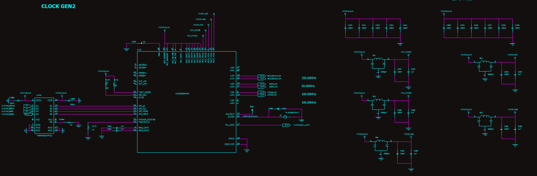
I have XTAL 25MHz at my only input clock source. And my register setting is as below:
REGISTERS
0 68840320
1 EB060321
2 EB260302
3 EB140303
4 68060314
5 10008B25
6 94BE03E6
7 FD91FDF7
8 80001A08
PORTS
0 FD
1 FF
2 DF
3 F9
INPUTS
PRI 25
SEC 0
AUX 25
EXTERNAL COMPONENTS
C4 1
R4 1
C5 1
My desired outputs are: CH1: disable; CH2: 100MHz (LVDS); CH3: 20MHz (LVDS); CH4: 41.67MHz (LVDS); CH5: Disable; AUX_OUT: 20MHz
(after writing these values to the chip; I read back all the values and they were all written correctly; also, I did trigger calibration bit after each registers writing to make sure the VCO got calibrated)
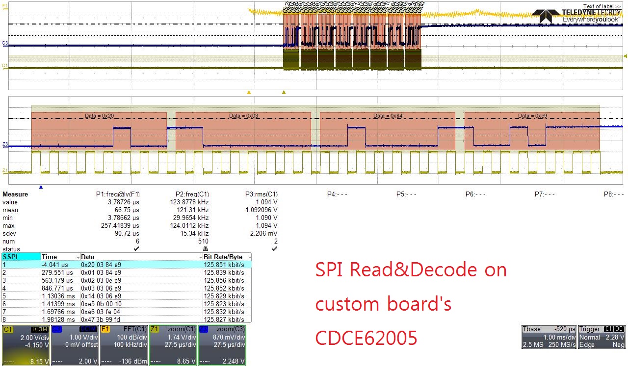
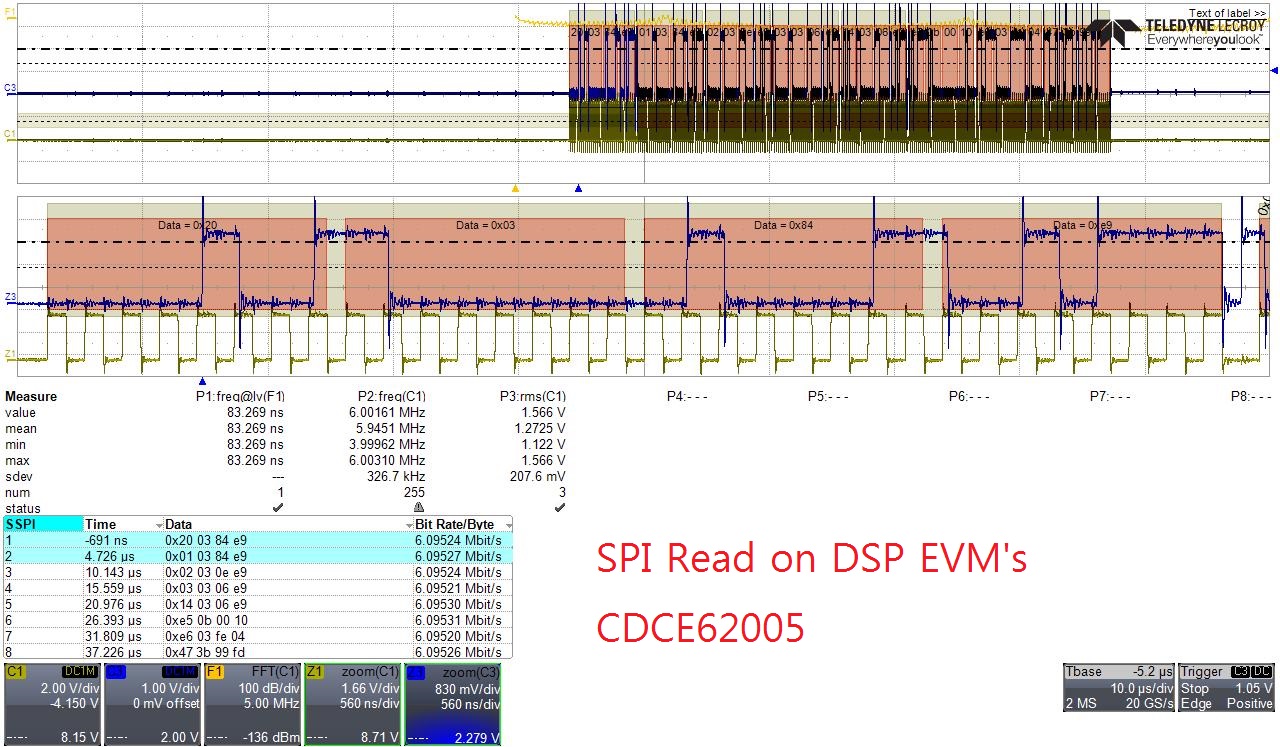
However, when I check the output with DSO; they are as follow:
CH1: disable; CH2: 250MHz; CH3: 50MHz;CH4:104MHz; CH5: disable; AUX_OUT: 50MHz.
Which means that all output got x2.5 multiplied compare to my desired values.
Also, the PLL LOCK pin is not active; when I change the detect window from 3.4ns to 28.6ns, the pin keeps toggling at all time.
Please let me know what is the cause of the issue and hopefully some hints to help resolve the problems.
Besides, I also noticed that the default register values I read back from a brand new chip are not the same as values described in the datasheet, is it normal or the chip got damaged, or something else?!
Thank you!