


Hi Team,
Could you please help to double review the schematic design of LMK00301? Especially for the output pin 9 and 10, it is HCSL to LVDS and input clkin0 pins. Thank you.
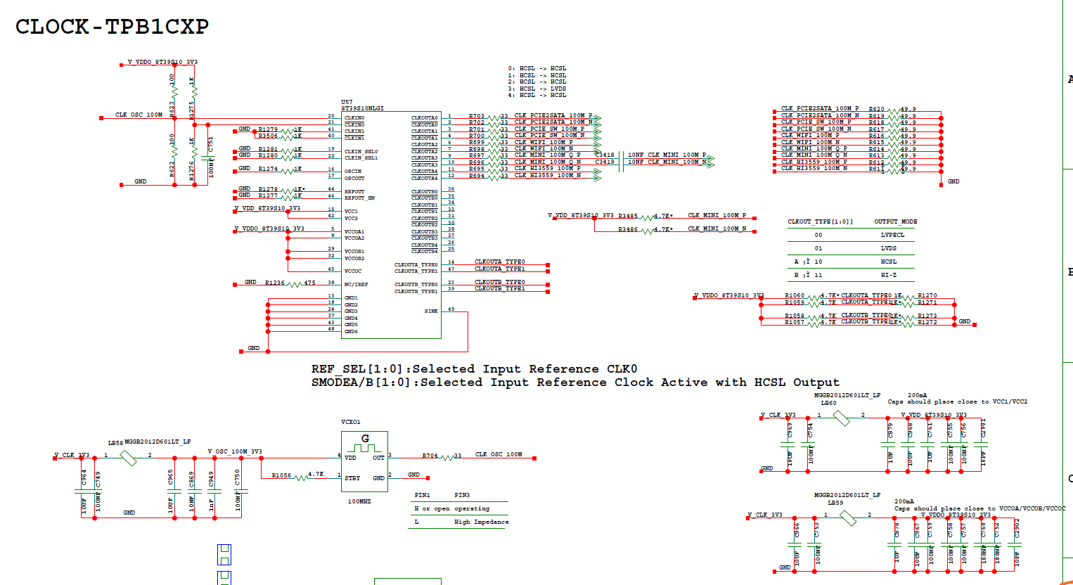
Hi Team,
Could you please help to double review the schematic design of LMK00301? Especially for the output pin 9 and 10, it is HCSL to LVDS and input clkin0 pins. Thank you.
