This thread has been locked.

If you have a related question, please click the "Ask a related question" button in the top right corner. The newly created question will be automatically linked to this question.

LMK04131: Reference clock

Part Number: LMK04131
Other Parts Discussed in Thread: LMK04133

Hi

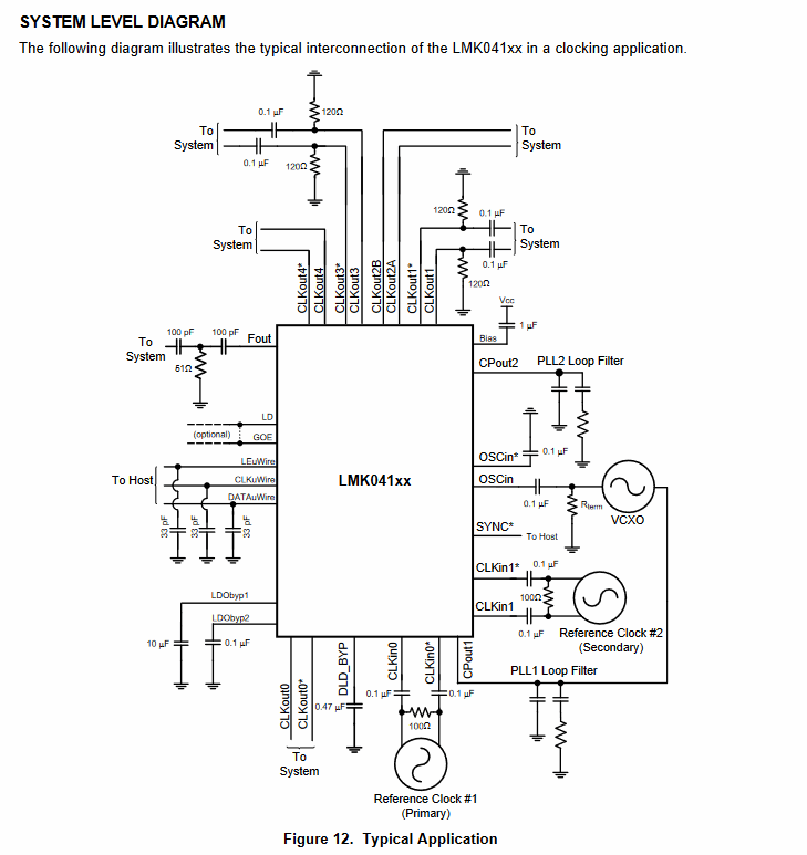
I have a question regarding the clock inputs to the lmk04131.

I do not know how to choose the values of the VCXO connected to the OSCin and the VCO connected to the reference clock CLKin0/1

I need 160 MHz and 320 MHz output. I would like to know how to determine the input frequencies. 

Regards Michelle

  • Hello,

    The LMK04131 is a jitter cleaner. This is typically used with an existing input from a recovered clock, but also if your reference frequency is low or doesn't relate well to the output frequencies resulting in a low phase detector frequency. Low phase detector frequencies can result in non-optimized PLL noise.

    If you just want 160 MHz and 320 MHz outputs, then you can bypass the first PLL of a dual loop device like LMK04131 or use a device without dual loop capabilities. The frequency you should pick is one that divides nicely into 160 and 320 MHz. So frequencies like 20, 40 or 80 MHz could be good candidates for an input frequency.

    Please refer to this presentation on choosing PLL loop bandwidths. It also illustrates further the impact of different phase detector frequencies of the PLL which could be forced by different reference frequencies.
    e2e.ti.com/.../664163

    Also, please see http://ti.com/clockarchitect
    This tool allows you to type in your needed input/output frequencies. Once in the tool there is a checkbox to automatically recommend input frequencies.

    73,
    Timothy
  • Hi

    The pdf is great, thank you so much.

    just a remark; the lmk04131 was recomented to by in another post, based on my application. I am just not sure how to set it up.

    My problem is that I am running a DAC and an ADC from an FPGA through a low pin Count FMC, so I have a very limited amount of clock pins available. I have 3 differential pairs but it would be beneficial for my design only to use 2. I need 1 for syncronizing the data coming back from the ADC and 1 coming from the lmk04131 to sycronize the data going to the DAC.

    As mentioned I do have a 3rd one to use as reference clock to the lmk04131 but I would really like to use that FMC pin for data transfer.

    If I bypass the first PLL as you mention does that mean I don't need a reference clock, just the external VCXO for the second PLL or do I need a reference clock no matter what?

    I tryed the clock architect simulation and apparently I cant use the lmk04131 but with the lmk04133 it Works. It suggests the internal VCO to 1920MHz and a reference input of 19.2MHz. But that does not divide into an even number with the 160 and 320 MHz signals. It does not say anything about the value of the external VCXO eather.

    I do not understand your first remark. Do I only need a jitter cleaner device if the reference signal comes directly from the FPGA? If I look at the datasheet for the lmk04133 the system diagram looks like this

    Here the reference clock is generated from a VCO. Is that the one that should be divided into an nice even number?

    Regards Michelle

  • I suppose FPGA is on one side of FMC, we called FPGA board.
    DAC, ADC & LMK041xx are located in another side of FMC, we called AFE board.
    First, we should decide how many clock domains are needed.
    If FPGA can have an individual clock domain for ADC and DAC data process, then a clock from LMK041xx is enough.
    AFE board can have a local XO as LMK041xx's reference. The XO is on LMK041xx OSCin. LMK041xx runs in PLL2 only mode.
    The XO frequecy could be 20 MHz, 40 MHz, 80MHz. 25 MHz XO would be worse than previous options.

    If FPGA must run in one clock domain, means all operations in FPGA are synchronized, then LMK041xx should get a reference from FPGA.
    LMK041xx must run in dual pll jitter cleaner mode . Then we need a VCXO on OSCin pins.