This thread has been locked.

If you have a related question, please click the "Ask a related question" button in the top right corner. The newly created question will be automatically linked to this question.

CDCE913 Output Problem

Other Parts Discussed in Thread: CDCE913

Dear All,

I've got a problem with CDCE913  output. The output frequency of CDCE913 doesn't equal the value I set and expect by setting EEPROM registers.

There is one 27Mhz Crystal(DSX530GA-27.000MHZ) in my design, and I select VCXO as clock input  to use PWM signal to control CDCE913. I want to generate  49.152Mhz frequency . But in result I got 49.1578Mhz  which can't  be accepted.


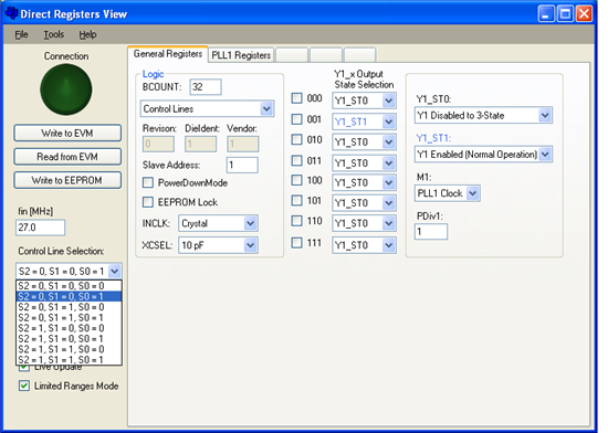
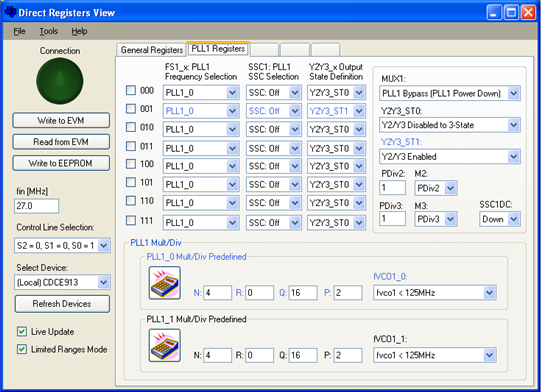
     I set up device  by software TI Pro Clock and I checked them a couple of times and they seemed OK.

:01000000817E
:0100010005F9
:0100020034C9
:0100030001FB
:0100040002F9
:0100050050AA
:0100060040B9
:0100070000F8
:0100080000F7
:0100090000F6
:01000A0000F5
:01000B0000F4
:01000C0000F3
:01000D0000F2
:01000E0000F1
:01000F0000F0
:0100100000EF
:0100110000EE
:0100120000ED
:0100130000EC
:010014004D9E
:0100150002E8
:0100160004E5
:0100170000E8
:01001800D611
:01001900D115
:01001A00E302
:01001B00AB39
:01001C0000E3
:01001D0040A2
:01001E0002DF
:01001F0008D8
:00000001FF

     The input Crystal  is 27.00003Mhz.
     The temperature of the the whole board is normal.

So what can cause this wrong output frequency?


Thank you for the suggestion.

  •  

    The CDCE913 has internal capacitors that you can program to match the crystal load specified by the XTAL datasheet. Therefore you might not need the external caps C80 and C81 that currently are in your schematic. That will fine tune the frequency of oscillation according to the pullability of the XTAL chosen.


    But I understand that you would like to control the frequency via Vtr and use the CDCE913 as a VCXO. In that case it is important to pay attention at the pull ability of the XTAL. Usually the pullability of the XTALs is less than +/-40ppm unless requested to the XTAL vendor, so more pullability can be achieved.


    The maximum pulling range is referring to the maximum possible change of frequency caused by the control voltage. Pulling range depends on the selected XTAL. i.e. a pulling range of +/-150ppm was measured for a CDCE9xx device. Vctr will vary the frequency of the VCO depending of the pullability of the XTAL selected. For more information on how to select the XTAL for maximum pullability go to the post (http://e2e.ti.com/support/clocks/f/48/p/56234/200872.aspx#200872).

    You might be interested in taking a look to the application note: SCAA088, that can be found in the link below:

    http://focus.ti.com/general/docs/techdocsabstract.tsp?abstractName=scaa088

    http://www.ti.com/litv/pdf/scaa085


    In the following application note you can see the CDCE913 used as VCXO http://focus.ti.com/lit/an/scaa088/scaa088.pdf


    You can find an additional article in the E2E forum:


    http://e2e.ti.com/support/clocks/f/48/p/56234/200872.aspx#200872


    Please let me know how can I further help you,

  • Hi

    Thanks for your help. I adjusted the crystal load and that's ok.

    Another problem, can I write 8 different setups for 8 output selection into the EEPROM at the same time?

    I'm going to use external control pins to select 8 different output and how should I save the predefined values to EEPROM?

    Look forward to your answer. Thank you!


    Best regards,


  • I would suggest you to write first the configuration you would like to have first.

    You can generate easily the configuration by using the followign software:

    http://www.ti.com/litv/zip/scac119b

    When executed, skip the wizard and go the main window. In the menu bar, select Tools>Direct register view

    Please note that in the control line selection combo is the control pins configuration and will set to blue the active setup for that selection. i.e. in this case when selecting S2=0, S1=0, S0=1, that will make active the Y1_ST1 selection that looking at Y1_ST1 combo box implies Y1 enabled. Also the PLL settings selected are the ones of PLL1_0 settings, as well as the SSC:off and Y2Y3 output stage definition is equal to the one defined in Y2Y3_ST1 that looking at its combo box selection is Y2/Y3 enabled.


    Once your setup in written then you need to configure the device so S0, S1 and S2 work as control pins, in order to achieve that:  the SPICON bit (bit 6 on byte 2) needs to be set to 1, and then that stored to the EEPROM by writing (1 in bit 0 of byte 6) .

    After writing the SPICON bit and saving that into the EEPROM. I2C communication would be possible when Vddout=GND and the two last bits of the slave address are set to 00. In this mode it is possible setting SPICON back to 0 when saved into the EEPROM (write 1 in bit 0 of byte 6). After this writting  I2C communication can be carried out as normal. 

    You can find more information about this in the application note:

    http://www.ti.com/litv/pdf/scaa105