This thread has been locked.

If you have a related question, please click the "Ask a related question" button in the top right corner. The newly created question will be automatically linked to this question.

LMK00301: Question about application scenario

Part Number: LMK00301

Hi team,

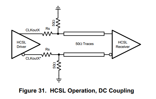
     Customer is evaluating LMK00301 device, could you please help to check the simplified block diagram as below? Thanks a lot! In addition, LVCMOS input has several options, which one has minimum jitter? Finally, please help to provide the recommended Rs value in Figure 31. Thanks!

Best Regards

Zhengquan Lu

  • Zhengquan,

    Based on figure 25, on page 22 of the datasheet, it suggests to me that perhaps the input signal should be AC coupled to allow the proper DC bias level. I know of nothing to suggest that there is a difference in jitter between CLKin0 and CLKin1 or P or N inputs.

    Regards,
    Dean