Other Parts Discussed in Thread: LMX2594,
|
Part |
Device-Pin |
Pin Name |
Signal Name |
Frequency MHz |
|
LMK04208 Input |
U90-36 |
OSC_IN_P |
OSCIN_4208_CMOS
|
122.880 |
|
LMK04208 Output |
U90-4 |
CLK_OUT0_P |
SYSREF_FPGA_C_P
|
Not Used |
|
LMK04208 Output |
U90-13 |
CLK_OUT1_P |
SYSREF_RFSOC_C_P |
250.000 |
|
LMK04208 Output |
U90-22 |
CLK_OUT2_P |
FPGA_REFCLK_OUT_C_P |
Not Used |
|
LMK04208 Output |
U90-48 |
CLK_OUT3_P |
LMX2594A/C_SYNC |
122.880 |
|
LMK04208 Output |
U90-53 |
CLK_OUT4_P |
REFIN_2594A/C_P |
122.880 |
|
LMK04208 Output |
U90-58 |
CLK_OUT5_P |
CLK_4208_OUT5 |
10.000 |
|
LMX2594RHAT Input |
U102-8 |
OSCIN_P |
REFIN_2594A_C_P |
122.880 |
|
LMX2594RHAT Output |
U102-23 |
RF_OUTA_P |
RF1_CLKO_A_P |
250.000 |
|
LMX2594RHAT Output |
U102-19 |
RF_OUTB_P |
RF1_CLKO_B_P |
250.000 |
|
LMX2594RHAT Input |
U104-8 |
OSCIN_P |
REFIN_2594C_C_P |
122.880 |
|
LMX2594RHAT Output |
U104-23 |
RF_OUTA_P |
RF3_CLKO_A_P |
250.000 |
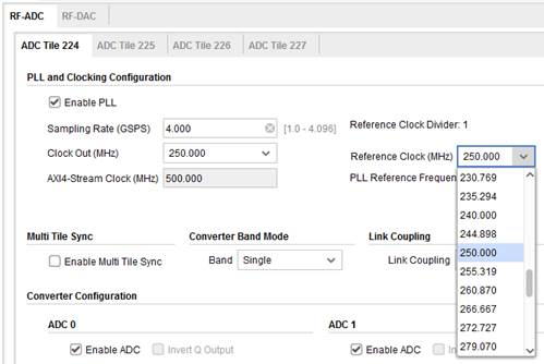
1. 1. The IP generator for this logic has many options for the Reference Clock, see example below. This same reference is also used for the DACs. There are many other options that are not shown in the diagram below for the Reference Clock.
2. 2. The TRD example reference design from Xilinx for this board clocked the ADCs at 4.096GHz, it used a Reference Clock of 245.760MHz. I was able to get the WebBench tool to find a solution. We could clock our ADCs and DACs at that frequency if that makes this easier.
|
Part |
Device-Pin |
Pin Name |
Signal Name |
Frequency MHz |
|
LMK04208 Input |
U90-36 |
OSC_IN_P |
OSCIN_4208_CMOS
|
122.880 |
|
LMK04208 Output |
U90-4 |
CLK_OUT0_P |
SYSREF_FPGA_C_P
|
Not Used |
|
LMK04208 Output |
U90-13 |
CLK_OUT1_P |
SYSREF_RFSOC_C_P |
250.000 |
|
LMK04208 Output |
U90-22 |
CLK_OUT2_P |
FPGA_REFCLK_OUT_C_P |
Not Used |
|
LMK04208 Output |
U90-48 |
CLK_OUT3_P |
LMX2594A/C_SYNC |
122.880 |
|
LMK04208 Output |
U90-53 |
CLK_OUT4_P |
REFIN_2594A/C_P |
122.880 |
|
LMK04208 Output |
U90-58 |
CLK_OUT5_P |
CLK_4208_OUT5 |
10.000 |
|
LMX2594RHAT Input |
U102-8 |
OSCIN_P |
REFIN_2594A_C_P |
122.880 |
|
LMX2594RHAT Output |
U102-23 |
RF_OUTA_P |
RF1_CLKO_A_P |
250.000 |
|
LMX2594RHAT Output |
U102-19 |
RF_OUTB_P |
RF1_CLKO_B_P |
250.000 |
|
LMX2594RHAT Input |
U104-8 |
OSCIN_P |
REFIN_2594C_C_P |
122.880 |
|
LMX2594RHAT Output |
U104-23 |
RF_OUTA_P |
RF3_CLKO_A_P |
250.000 |
1. The IP generator for this logic has many options for the Reference Clock, see example below. This same reference is also used for the DACs. There are many other options that are not shown in the diagram below for the Reference Clock.
2. The TRD example reference design from Xilinx for this board clocked the ADCs at 4.096GHz, it used a Reference Clock of 245.760MHz. I was able to get the WebBench tool to find a solution. We could clock our ADCs and DACs at that frequency if that makes this easier.


