This thread has been locked.

If you have a related question, please click the "Ask a related question" button in the top right corner. The newly created question will be automatically linked to this question.

NE555: Time delay between the Vout and power supply

Part Number: NE555

Hi Team, 

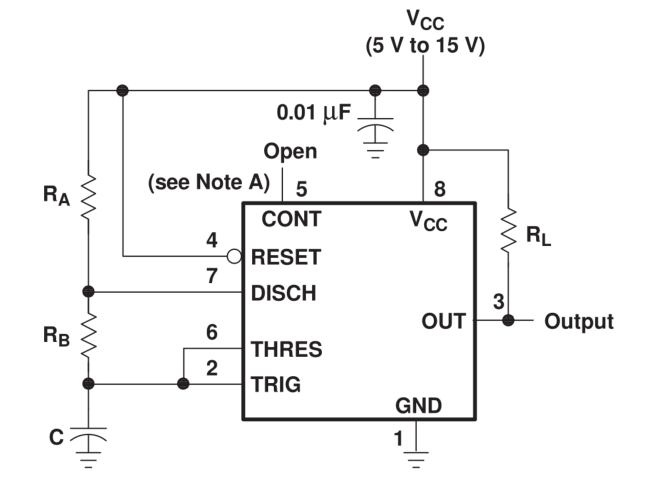
NE555D is used to design a circuit for astable operation as shown in the picture. When Vcc is powered on, the OUT pin goes high. My question is:

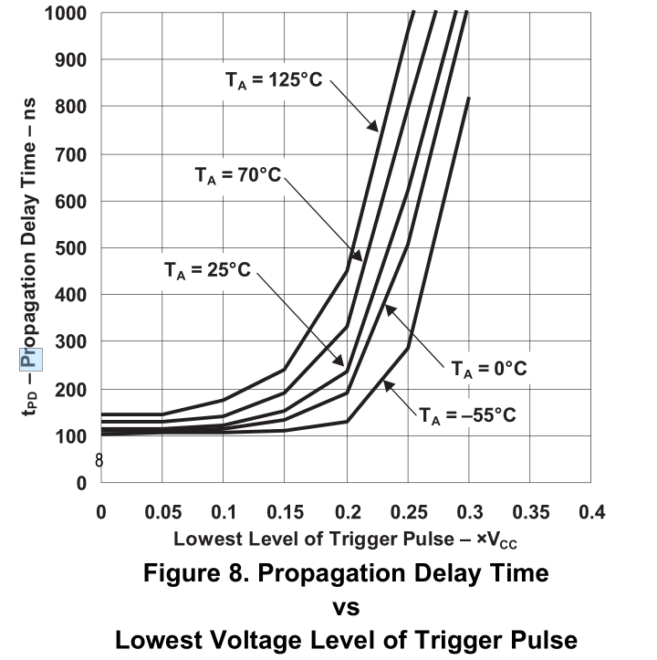
What's the time delay between the OUT going high and Vcc powered up? It's much the same as the propagation delay of the device.

Thanks and Best Regards!

Hao

  • Hao,

    The output should be high within propagation delay or immediately. Because "C" starts at 0V, the first output high time will be longer. The following output high times start at "C" at 1/3 Vcc
  • Hi Ronald,

    Thanks! The figure 8 in the datasheet has the propagation delay. What does the "lowest voltage level of trigger pulse" mean?

    Thanks and Best Regards!

    Hao

  • Hao,

    This chart assumes a square wave input signal so lowest level is the VIL, voltage input low level. For an a-stable setup, trigger falls over time so the response uses a range of the curve, not just one point.

    For very low frequency the switch happens at 0.33 as the voltage falls very slowly , but the long propagation delay doesn't matter.
    For low frequency the switch happens just under 0.33 as the voltage falls slowly, but the lower voltage improves propagation.
    For moderate frequency (<10kHz) the switch happens near 0.3 as the voltage falls faster, but the even lower voltage improves propagation.
    For higher frequency (>10kHz) the switch happens under 0.3 and the simple data sheet formulas will show faster than reality results because the timer is now passing the 1/3, 2/3 thresholds which adds to the charge and discharge times.