This thread has been locked.

If you have a related question, please click the "Ask a related question" button in the top right corner. The newly created question will be automatically linked to this question.

CDCLVC1310: Schematic review and The GND connection

Part Number: CDCLVC1310

Hi team,

Can you help to review below schematic.

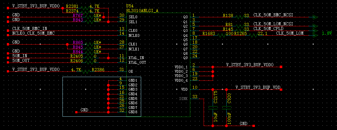
For the CDCLVC1310, can we connect all the GND pin together as below:

Lacey

Thanks a lot!

  • Hi Lacey,

    Some feedback:
    -The XTAL is not shown in the schematic, but it is selected with IN_SEL[1:0]. Place the XTAL close to XTAL_IN / XTAL_OUT.
    -Assumed that PRI_INP / PRI_INN input termination is OK.
    -Recommended to place 0.01uF and 0.001uF decoupling capacitors on each VDD and VDDOx pins near the device.
    -It seems that Q4 is being level translated to 1.8V. I assume this is OK. Be aware that impedance mismatches will degrade signal integrity. The other clock outputs are OK.
    -Connecting all the GND pins is OK.

    Kind regards,
    Lane