A related question is a question created from another question. When the related question is created, it will be automatically linked to the original question.
If you have a related question, please click the "Ask a related question" button in the top right corner. The newly created question will be automatically linked to this question.
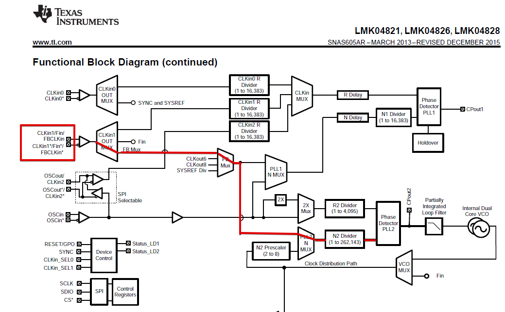
The path you highlight is intended for use as a PLL feedback path, it would normally be used to perform 0-delay by routing an output clock back to PLL2 through an external path -- which for most purposes you can do more simply using CLKout6 or CLKout8 for 0-delay feedback internally.
While you could technically use this path for a reference, then route an output clock into OSCin to provide a feedback path (and effectively flip PLL reference and feedpath paths) - you wouldn't want to do this because it would break the VCO calibration.
If you require a method to connect CLKin1 to PLL2 reference, please consider the pin compatible and programming similar LMK04832. This allows CLKin1 to be connected to PLL2 reference. Note that output formats are a bit different between LMK04828 and LMK04832. This is really convenient on LMK04832 because these CLKin1 pins can be used as reference to PLL1, reference to PLL2, or clock distribution.