This thread has been locked.

If you have a related question, please click the "Ask a related question" button in the top right corner. The newly created question will be automatically linked to this question.

LMK04828: Synchronizing CLKouts of two LMK devices

Part Number: LMK04828

Hello,

I have two LMK04828 devices that I need to sync in order to have deterministic phase relation. Below are some questions I couldn't find answers to in the datasheet.

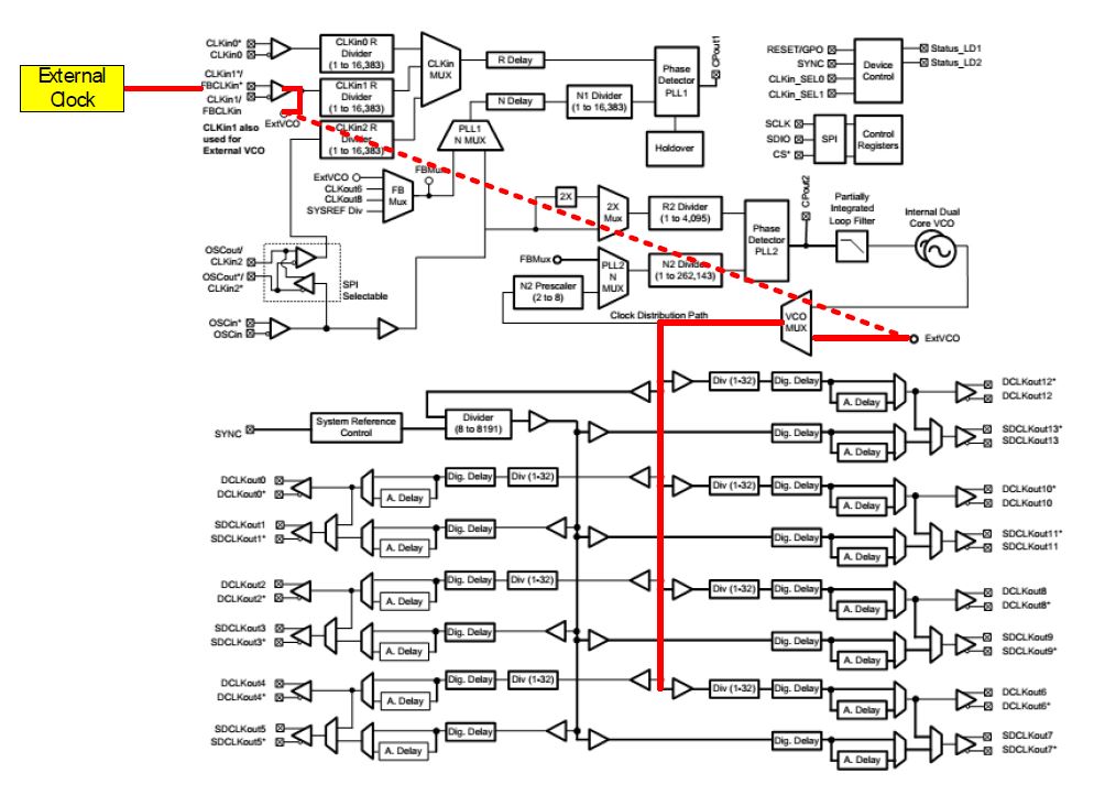
1. Within one LMK device, are the divided down, CLKout's Phase locked to the OSCin. Per the block diagrams, I notice there are VCO's that I assume multiply up the input before it gets divided down to the CLKout value. So, I wonder if all the divided down values are locked to the OSCin or locked to the VCO internally. 

2. When using the SYNC pin as the source for the SYNC Input to the LMK device, does it need to be synchronous to the OSCin. Register 0x143 allows you to configure the Sync_1shot_en as edge sensitive, but to what edge is that edge sensitive input sampled at? Or is it asynchronous reset to the dividers?

Thanks!

  • Hello Roy,

    1. Within one LMK device, by default the CLKout signal phase is locked to the VCO, so all the delay components introduced by dividers are distinct. Normally, this means the CLKout signal has no deterministic relationship with the OSCin signal. However, using 0-delay mode (datasheet 9.1.11) you can establish a deterministic phase relationship between an output clock signal and the OSCin signal by internally feeding one of the CLKout signals to the phase detector. The rules for generating a deterministic phase relationship are:
      1. GCD(OSCin, CLKout) = OSCin; greatest common divisor between OSCin and CLKout should be OSCin. Substitute OSCin with CLKin for nested 0-delay.
      2. If multiple outputs require determinism, the feedback frequency must be GCD(CLKout0, CLKout2, ... CLKoutX). This means that the 0-delay feedback frequency will be the lowest output frequency used.
    2. What clock samples the SYNC input can differ depending on how synchronization is set up, especially when syncing multiple devices.
      1. Sampled to distribution path frequency: this is the default in most cases. It can be difficult to synchronize to a distribution path frequency, especially when the source is a VCO is operating at several GHz. Using the SYNC pin, this is likely not possible due to variations in the setup and hold times across temperature and supply voltage. On the other hand, using the LMK04828 in distribution mode, this can work very well (especially if the frequency at CLKin1 is low). From your use case, it does not sound like this option is available.
      2. Sampled to SYSREF frequency: By selecting CLKin0 to be the source for the synchronization signal, even if it is only a single pulse, and by using the SYSREF path as the source in the FB_MUX, it becomes possible to expand the window for a synchronization event from several hundred picoseconds to several nanoseconds, which is a more plausible target to hit. The SYSREF divider output frequency must be at the phase detector frequency, or must divide down evenly to the phase detector frequency using the N-divider. The CLKin0 pulse will be re-clocked to the SYSREF edge, which is phase-locked to the OSCin frequency. The CLKin0 path delay is almost invariant across operating temperature and frequency, and this gives >1ns window for most OSCin frequencies below about 250 MHz (and the window gets larger as OSCin frequency is reduced).

    Regards,

  • Hi Derek,

    Thanks for the reply. Currently, I have both LMK devices in External Clock mode so that CLKin1 is feed to Fin and passed thru the VCO Mux to the System Ref Control and dividers per Figure 11 (LMK04828 Block Diagram) bypassing the VCOs. Basically, I am using the Ext Clk directly in both devices. DCLKout2 to a DAC and DCLKout4 to an ADC are set to divide by 1. DCLKout8 is divide by 4. This is the clock on both devices that I need to sync since I see phase variations between the DAC outputs associated with the two LMK devices. 

    I planned to use the DCLKout0 output divided by 32 from one LMK device as a slow clock master to send a signal to each LMK's sync pin rather than configuring each device to use the CLKin0 as the sync. Does this sound like a possible solution?

    Thanks,

    Roy.

  • Hi Roy,

    Sorry for the delay. I think this will depend on the frequency being fed to the second LMK04828 in the chain. For lower frequencies (<250 MHz) the SYNC pin timing window will likely be large enough that this should be doable. For higher frequencies, passing the SYNC signal through CLKin0 sees much lower overall variation across temperature and supply voltage, so precise timing windows are easier to hit. This is not to say that they can't also be hit precisely with the SYNC pin, but it may require some calibration to ensure that the SYNC signal is timing the right external clock edge over temperature and supply voltage.

    Regards,