Other Parts Discussed in Thread: DS280DF810
Hi,
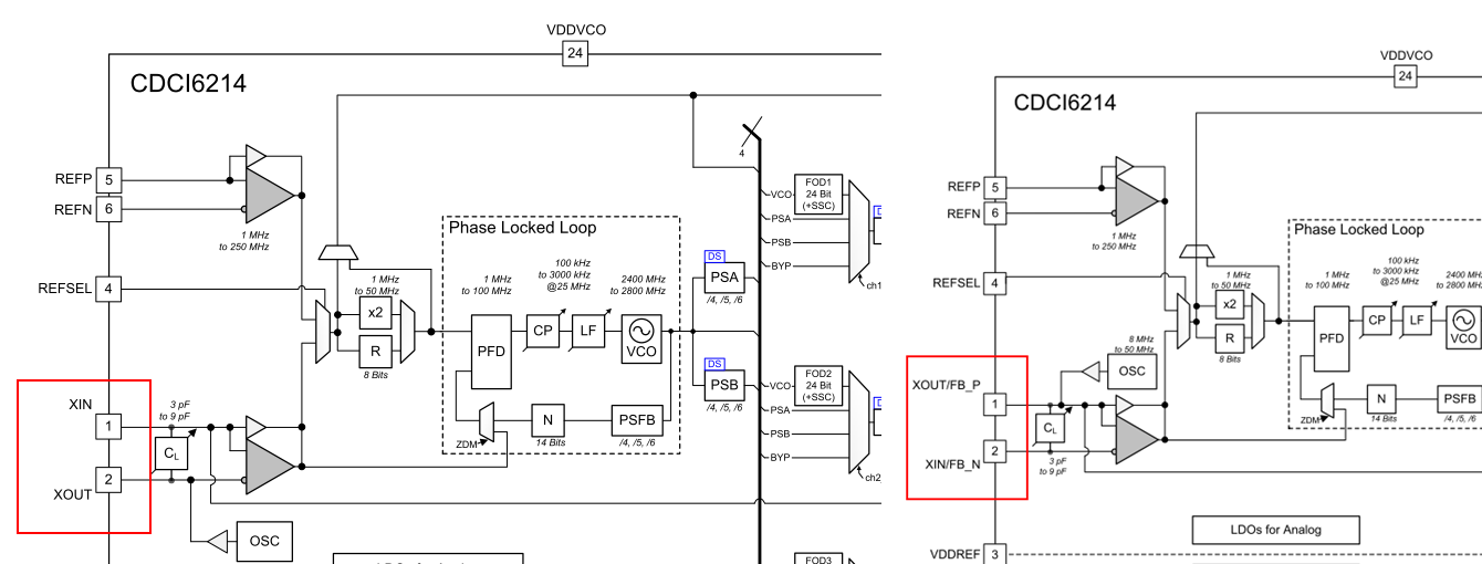
1. Picture1 show the old and new function block diagram. We noticed pin1 and pin2 name be swapped,whether or not it just correct the pin name and the chip die is the same.
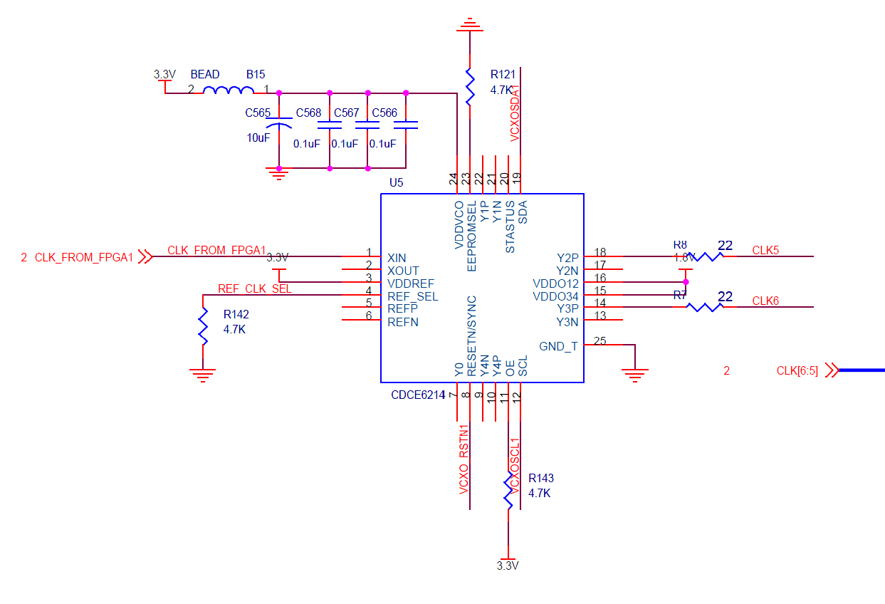
2. Picture 2 is customer's schematic , Is it ok if PIN1/REFP as single end clock input?
Thanks