This thread has been locked.

If you have a related question, please click the "Ask a related question" button in the top right corner. The newly created question will be automatically linked to this question.

LMK04208: External VCO mode

Guru 19785 points
Part Number: LMK04208

Hi Team,

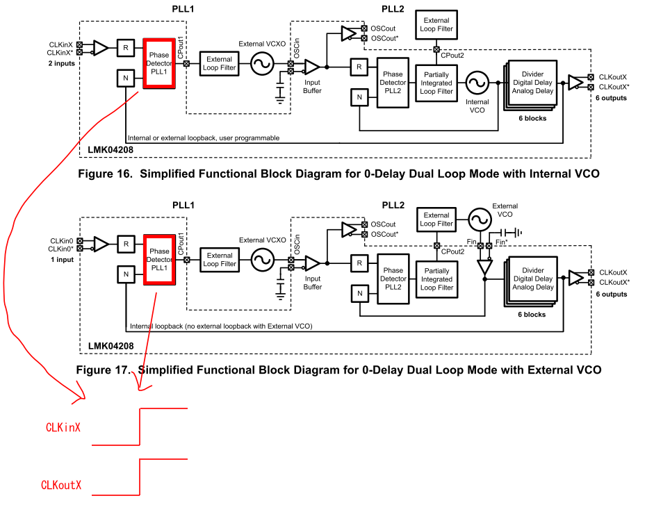
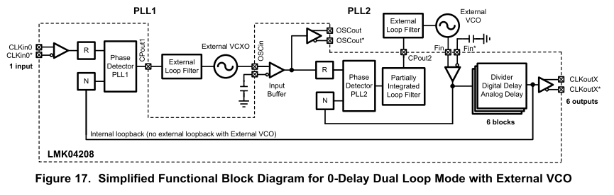
In the LMK04208 datasheet, there is below description for external VCO mode.

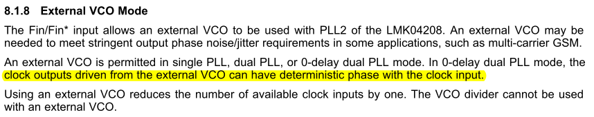
I couldn't understand why there would be deterministic phase difference between clock input and VCO feedback clock in 0-delay mode.
Could you elaborate for this description ?

As long as used in 0-delay mode, connecting the clock output to the PFD, I think both phase are synchronized.

Best Regards,
Kawai

  • Hi Kawai,

    VCO feedback clock is necessarily in phase with PLL2 input as you said. But some customers have asked if 0-delay depends on internal propagation delay, and whether the output-to-input phase determinism provided by 0-delay is only available using the internal VCO, since external VCO would have much more propagation delay which adds phase lag to output phase with respect to input phase. We wanted to make it clear that 0-delay mode is available independent of VCO propagation delay, and that the clock outputs can still have deterministic phase with the clock input.

    Regards,

  • Hi Derek-san,

    I couldn't understand your explanation.

    Whether there is a probagation delay in the VCO itself or trace length at the external VCO circuit, PFD should align the phase between the input frequency and the output frequency. That is my understanding how PLL works.

    How could the behavior change between the internal VCO and external VCO ?

    It would be helpful if you could explain in specific.

    Thanks and Best Regards,

    Kawai

  • Hi Derek-san and Team,

    Could you please help us answer customer ?

    Propagation delay may be different in the path from Phase Detector and N divider, however, we believe 0-delay could be achieved even with in external VCO mode.

    Best Regards,

    Kawai

  • Hi Kawai-san,

    Apologies for the delay, I fell ill for some time.

    To be clear: 0-delay can be achieved even with external VCO mode. 0-delay behavior should not change between internal and external VCO mode. VCO propagation delay variation does not impact 0-delay mode.

    I think the clarifying sentence in the datasheet was included for two reasons:

    1. Some customer did not understand 0-delay mode, and asked if there was any effect due to propagation delay
    2. CLKin1 can be used as both 0-delay feedback (FBCLKin) or as external VCO (Fin) depending on mode settings, so some customers may assume that there is no 0-delay feedback path in external VCO mode

    As you stated, PFD should align the R and the N paths regardless of VCO propagation delay. And Figure 17 shows that there is an internal 0-delay feedback path, so 0-delay can be used in external VCO mode.

    Regards,

  • Hi Derek-san,

    Thanks for the support.

    I understood that 0-Delay could be achieved with both internal and external VCO mode.

    So what is the object of describe this statement in the datasheet ?

    "clock outputs driven from the external VCO can have deterministic phase with the clock input"

    I still cannot understand why there could be deterministic phase between the input clock and external VCO clock output.

    Best Regards,

    Kawai

  • Kawai-san,

    "Clock outputs driven from the external VCO" means the clock outputs that get divided down from the VCO feedback clock, and not the VCO feedback clock itself. The VCO feedback clock will not have a stable phase relationship with respect to the reference clock input.

    Regards,

  • Hi Derek-san,

    Thanks for your continuous support. However, I am confused again.

    Do you mean that following Figure 17 cannot achieve 0-delay if the output divider is set to >2 ?
    I still cannot understand why there could be phase difference here.

    I am understanding that there could be phase difference in the following PLL design (Figure 18), because the output divider is not included in the VCO frequency feedback loop when divider value is >2.

    Is this what you meant ?

    Best Regards,

    Kawai

  • Hi Kawai-san,

    Sorry that my explanation has not been very clear.

    When in 0-delay mode, whichever output clock is used as the N-feedback will be in phase with the reference clock input. This is true regardless of the output divider or N-divider settings, as long as phase detector sees the same frequency at both inputs. So both Figure 17 and Figure 18 can achieve 0-delay, and the divide value may be any value which satisfies the phase detector frequency.

    Because of digital delay, analog delay, or divider reset/SYNC feature, the phase relationship between the output clocks (and therefore between the output and input clocks) will not always be the same. However, because all output clocks are derived by integer division from a common VCO clock, the number of different phase offsets between outputs is limited (deterministic). Since all outputs have a determistic phase relationship between each other, and one output is known to be in phase with the input clock, therefore all clock outputs driven from the VCO can have a deterministic phase relationship with the input clock in 0-delay mode. This is true regardless of whether internal or external VCO is used. Unless the VCO frequency is also the phase detector frequency, the actual phase of the VCO with respect to the input clock does not impact the deterministic phase relationship between clock inputs and clock outputs in 0-delay mode.

    When not in 0-delay mode, the propagation delay of the channel dividers varies differently from the propagation delay of the N-dividers. So if 0-delay mode is not used, there is no way to guarantee a deterministic phase relationship between the clock input and the clock output.

    Regards,

  • Hi Derek-san,

    Sorry that I had chosen the wrong picture, Figure 18. Output divider was inside the feedback loop that it could also achieve 0-delay.

    Please see the following figure.

    The device is designed as 0-delay mode. CLKout4 is used as PLL1 feedback. and CLKin and CLKout4 should be aligned.

    From you explanation, do you mean that there would be deterministic phased difference between CLKin and CLKout1 / CLKout2 / CLKout3, due to the propagation delay in each divider or delay block even if they are set as a same value ?

    Best Regards,

    Kawai

  • Hi Kawai-san,

    That is exactly what I mean.

    Regards,

  • Hi Derek-san,

    Thanks, I understood.

    I have one advise that this could be said to both internal VCO and external VCO.

    The datasheet describes as it is only applied to external VCO and that is why I was confused.

    Best Regards,

    Kawai