Other Parts Discussed in Thread: USB2ANY
Dear Sir:
About the LMK05318 used in our products, we are trying to program the internal EEPROM via the I2C interface.
Our products used the ARM CPU + Linux OS.
1) In the datasheet, Chapter 9.5.4, it said:
The register map data (hex format) or SRAM/EEPROM map data can be exported to enable host programming of the LMK05318 on start-up.
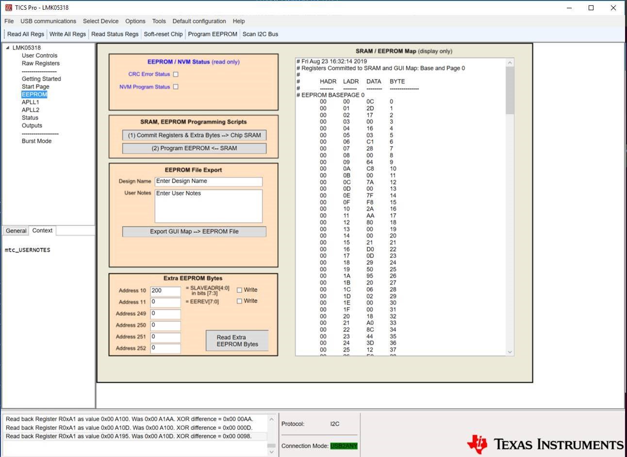
Q-1) Can the TICS Pro software tool generate the SRAM/EEPROM map data to be used for the programming of internal EEPROM?
Q-2) To program the internal EEPROM of LMK05318 with the SRAM/EEPROM map data, does TI provides the sample codes (command line tool) on Linux OS?
Thank you.
Best Regards.