This thread has been locked.

If you have a related question, please click the "Ask a related question" button in the top right corner. The newly created question will be automatically linked to this question.

LMX2581: How to read back LMX2581 register

Part Number: LMX2581

Hello,Noel

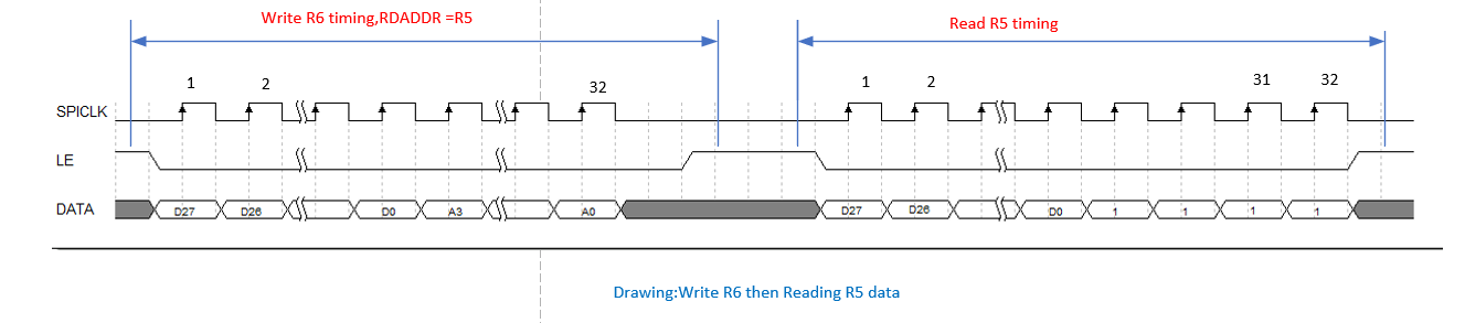
we are now configure LMX2581,We want to verify our SPI communication module through reading back LMX2581 register;

but we don't quite understand the reading back timing


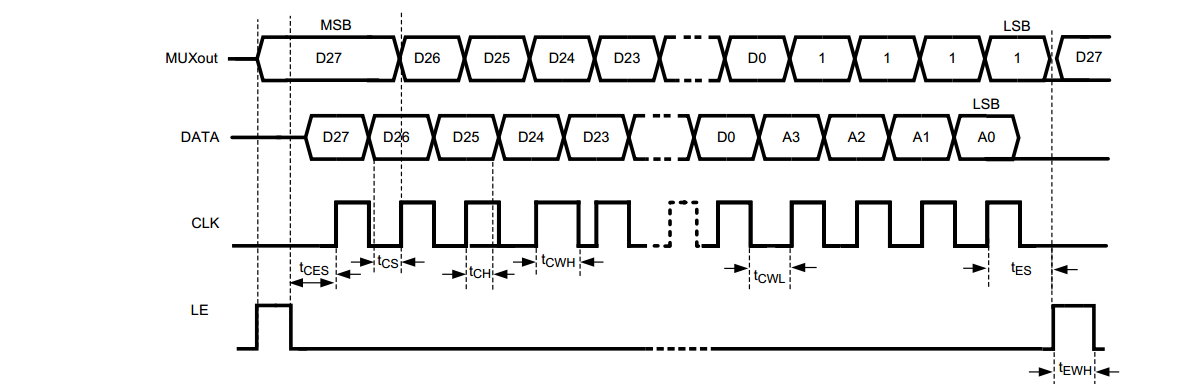
For normal SPI reading a register,we will first give the register address,then the  register data is coming out;But I don't understand the explanation about through reading R6 in datasheet.

could you give me a detailed explanation, It's better to give an example;rat aorta ring assay


Best Regards

  • Hello,

    First, setup the outputs are described in datasheet, e.g. MUXOUT_SELECT or LD_SELECT to readback mode.

    Now to get data form the MUXOUT or LD out pin... the datasheet is suggesting that you:

    Toggle LE high then low.  (Note this would reload the last register programmed).

    Then provide the 32 clocks to get all the data.  The data you read back will be the register specified by R6's RDADDR.  While clocking out the data, you will be loading the shift buffer such that when LE goes high again, that register loaded will be programmed.  R6 is recommended as a good register to program during readback.  The address of the readback will be defined by R6's RDADDR.

    I recommend you...

    1) Program R6 RDADDR with the address you want to readback, then.  After the LE goes high and returns low...

    2) Provide another 32 clocks to clocks out the data of the register specified by R6.  Each address bit will always clock out 1s.  So an address of 15  will be read.  While providing these clocks, the shift buffer is loaded with data.  So on the next LE, that data will be loaded.

       - If you want to readback all registers, each time you're "programming R6" to clock out the readback data, you can increment the RDADDR in R6.

    Note.  My understanding is that you if you don't give that last LE pulse, you will not actually program any register on readback.  However it is always true that the last 32 bits clocked into the shift buffer will be loaded on the next LE.

    73,
    Timothy

  • Hello,Timothy

                   Thanks for your help,now I tell you reading back LMX2581 register details;

    (1) we set SPI clock 2MHz

    (2)Firstly, we set R5's value is 0x01308005, then,we are reading R5's value through R6;

    (3)but,the reading data is not equal 0x01308005;

    (4)write r6 timing and then reading R5 timing is as below


    Timothy, Is our timing is ok? And,what's wrong with R5's data reading back?

    73,

  • Hello,Timothy

                   Thanks for your help,now I tell you reading back LMX2581 register details;

    (1) we set SPI clock 2MHz

    (2)Firstly, we set R5's value is 0x01308005, then,we are reading R5's value through R6;

    (3)but,the reading data is not equal 0x01308005;

    (4)write r6 timing and then reading R5 timing is as below

    Timothy, Is our timing is ok? And,what's wrong with R5's data reading back?

    73,

  • Hello,

    I don't see the exact timing, but yes.  It seems you are doing the correct thing.

    What do you read back?

    * If you leave the LE high after the R6 write with R5 address and just clock.  What do you then read?

    * Which pin are you reading back from?  What is MUXOUT_SELECT or LD_SELECT set to?

    * You have set MUXOUT_PINMODE or LD_PINMODE = Push-Pull?  Or if Open drain have an appropriate pull up resistor?

    73,
    Timothy

  • Hello,Timothy

             Thanks for your help,Now,I answer the above question;

      Q: * If you leave the LE high after the R6 write with R5 address and just clock.  What do you then read?

      A:  When leave the LE high after the R6 write with R5 address and just clock,Then read R5 data,I leave LE from high to low ,after providing 32 clocks then    leave LE high.

     Q:* Which pin are you reading back from?  What is MUXOUT_SELECT or LD_SELECT set to?

     A: We use  MUXOUT pin for reading back;MUXOUT_SELECT=Readback Data; LD_SELECT= DLD & Vtune Good

     Q:* You have set MUXOUT_PINMODE or LD_PINMODE = Push-Pull?  Or if Open drain have an appropriate pull up resistor?

    A: We set MUXOUT_PINMODE = Push-Pullor;LD_PINMODE = Push-Pull


  • Hi,

    Can you advise for both cases.  LE low, and LE high.  When you read back, you expect to read:

    0x01308005

    But you actually read what value?

    73,
    Timothy

  • Hi There,

    Here is a programming example, hopes it help.

    First of all, I have the EVM power up.

    Then I write all the registers once, this completes the initial power up programming. (R5 is 0x01308005)

    I do the following in order to read back R5.

    1. write R6 with RDADDR=5(decimal)

    2. write R6 with RDADDR=5(decimal)

    - MUXOUT is monitored

    Here is the MUXOUT waveform. I got the correct R5 reading.