This thread has been locked.

If you have a related question, please click the "Ask a related question" button in the top right corner. The newly created question will be automatically linked to this question.

LMK04828: LMK04828 Temperature Drift Issue

Part Number: LMK04828

Hi Team, 

My customer is using the LMK04828 for below evaluation scenario:

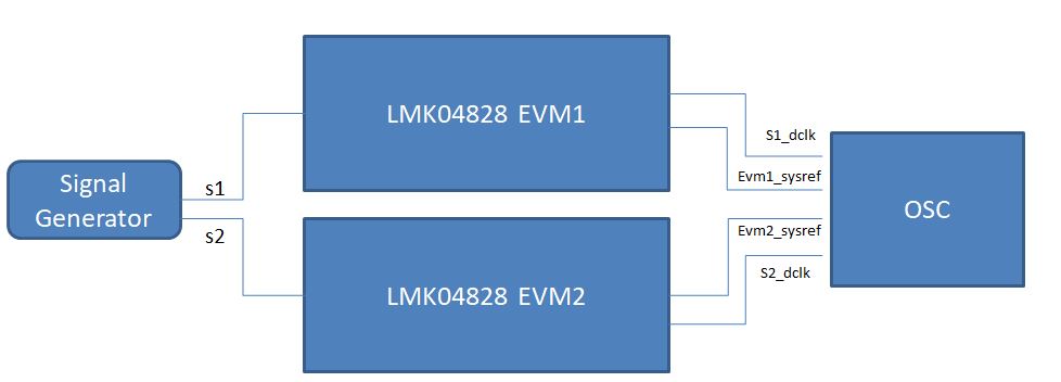
The S1 and S2 are from the signal generator and the same phase sine-wave signal, when testing, both LMK04828 EVMs are set at 0-delay mode. 

And when they're both in the room temperature, the output of the EVM1 and EVM2 have the same phase according to the result of the OSC. 

However, when giving the EVM2 30'c additional heat, that's 50~60'C, the output of EVM2's signal phase is not the same as the EVM1 in room temperature. Moreover, it was found that the output of the EVM2 phase is not the same as input S2. However, each of the EVM2's clock output's has the same phase output.

So it seems temperature drift would affect the output's phase shift comparing to the input, though the different output clocks on one signal EVM are the same.

Is this an expected behavior about the temperature drift?

If customer want the EVM1 and EVM2 get the same output phase as the S1&S2 when they're working in different temperature but within the normal working temperature range, what can we do with that? 

Expecting your response! Thank you!


  • Hello Steven,

    Are they using the LMK04828 in dual or single loop?  If using dual loop, are they using cascaded or nested 0-delay?

    Nested zero delay where the CLKin reference to the LMK04828 is compared to the output would result in the lowest variation input to output.  However in dual loop mode, the input impedance of the VCXO would also impact the input to output phase variation.  If using this, mode - one way to eliminate this could be to use an op amp to buffer the loop filter output so that the PLL charge pump sees a high impedance load and the leakage from the loop filter capacitor is small and deterministic.

        * If this is the case, can they advise if the VCXO input impedance is consistent over temperature?

    Single loop mode with OSCin input uses the internally well controlled input impedance of the integrated VCO.  In 0-delay mode for PLL2, I've measured a delta of 170 ps of variation input to output at 3.3 V.  If I include voltage variation, then the worst case increases to 290 ps.

    Just how much variation is the customer seeing?

    -

    If using dual loop, we do have the ability to use PLL1 R DLY and PLL1 N DLY register to shift the phases of input to output in approximately 200 ps steps.

    In either dual loop or single loop mode, you could also perform dynamic digital delay adjustments of the output clocks or the feedback clock to cause a phase shift of input to output to attempt to keep the phases aligned.

    73,
    Timothy

    73,
    Timothy