This thread has been locked.
If you have a related question, please click the "Ask a related question" button in the top right corner. The newly created question will be automatically linked to this question.
Hello!
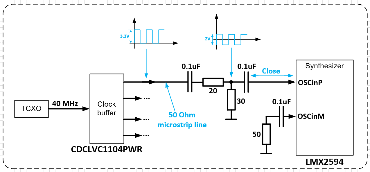
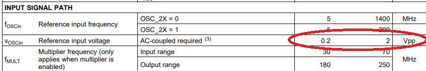
In our projects we use LMX2594 synthesizer. We want to connect the Single Ended reference clock to this synthesizer (to OSCinP pin). But what we must to do with OSCinM input? We can not to find the recommendation in datasheet. Please help us, how to correctly connect the Single Ended reference clock?
Thanks for posting on E2E. I have assigned your post to the responsible engineer. He will respond to you soon.
Kind regards,
Lane
Hi Artem,
We don't need the 20Ω and 30Ω resistors to voltage divide the 3.3V CMOS clock, when the buffer is driving a 50Ω load, the voltage swing will drop.
I recommend use the circuit as shown in the datasheet, Figure 10.
For the LMX2594 the ref. clock input voltage should be no more than 2Vpp according to sythesizer datasheet:
Therefore, I put a voltage divider from resistors 20/30 Ohms.
If we apply the option from Figure 10,
then the signal voltage swing will be 3.3 Vpp. It will not lead to failure of the LMX ref. input?
Perhaps I did not take into account something and am mistaken, tell me, please.
Hi Artem,
The VOH of the buffer will change according to the load current.
If the load is high impedance, load current is small, then VOH may reach 3.3V.
However, if the load impedance is small, VOH must drop to maintain a current flow.
Check datasheet Section 6.5, VOH will drop to 2.2V if the load current is 12mA.
Hi Noel,
Thank you. About the dependence of the VOH drawdown on the load resistance is understandable.
But what swing / amplitude will the reference signal have in your recommended circuit (at the ref. PLL pin)?
Will there be an excess of 2Vpp? Or vice versa, drop are too low ... I do not understand how to calculate this, based on the data in section 6.5.
I measured the 40MHz output swing with 50ohm load on my bench using CDCLVC1104EVM. For VDD = 2.5V, the output amplitude is 1V. For VDD = 3.3V, the output amplitude is 1.6V.
Kind regards,
Lane
Hi Lane,
thank you very much for the info. Please clarify, did you use such a scheme?
Can you recommend it for CDCLVC1104 + LMX2594?
Rather than the two 100ohm resistors, I just used the 50-ohm termination inside the scope. Also, there is no AC-coupling capacitor.
Yes, you can use this scheme to connect CDCLVC1104 and LMX2594.
Kind regards,
Lane
Hi Lane!
I also wanted to clarify one question. I did not immediately notice that you wrote about the 1.6V AMPLITUDE. The total signal swing will be twice as large, i.e. 3.2V. For a LMX2594 synthesizer, a maximum value of only 2 Vp-p is permissible. The buffer power is fixed at 3.3V (in our case). Which circuit in this case would you recommend to use for connection CDC buffer with LMX?
Hi Artem,
You can use this circuit, it should reduce the swing to 1.6Vpp for 3.3V supply for CDCLVC1104, which is less than the 2Vpp input limitation.
Kind regards,
Lane
We had the opportunity and today we measured the signal using such a circuit - we observed is approximately 3Vpp (amplitude 1.5V). The synthesizer was not connected, but it has a high-impedance input, it should not affect...
That is strange, I measured using an equivalent load and got half the swing. So the swing is not attenuated when you use the resistor divider versus open circuit? I would expect the load to have some impact.
Perhaps you could try replacing the resistor divider with a 50ohm termination to ground and see if the swing is attenuated for double confirmation.
This is the typical method to attenuate a signal while maintaining signal integrity (50ohm to GND at receiver). If you would prefer a dual supply device that is more easily configured for 1.5V/1.8V output level, you might be interested in LMK00804B instead.
Kind regards,
Lane