Other Parts Discussed in Thread: LMK04610
Hi,
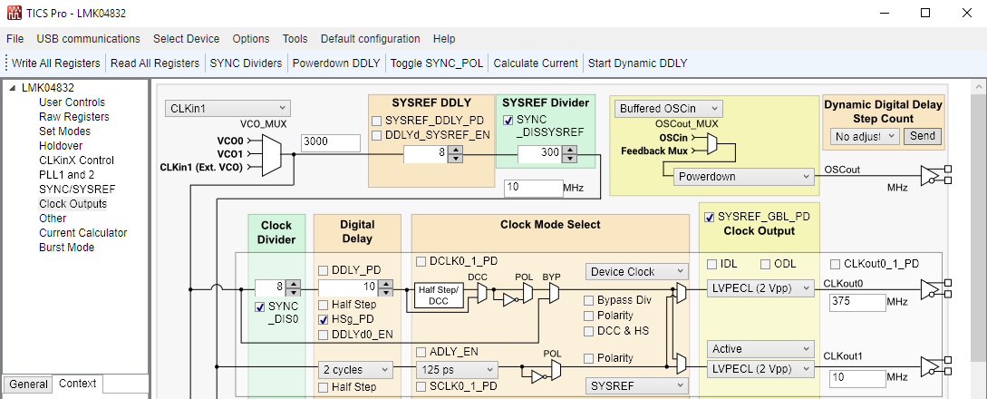
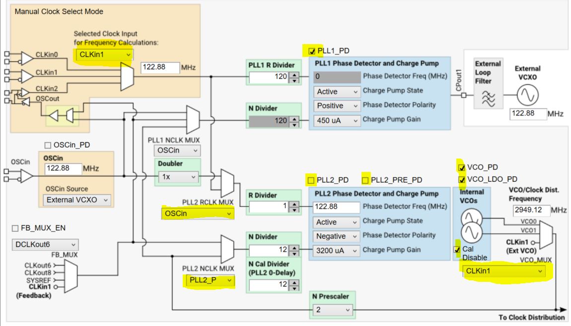
I'd like to use the LMK04832 (EVM) in external VCO/clock distribution mode but am not sure what I need to program on the CLKinX Control, PLL 1 and 2, and Clock Output pages on TICS Pro. Please see below more details on my application.
I am feeding a high frequency input clock to CLKin1 - a 1.25 to 3 GHz sine wave. I will need two device clock outputs from the LMK device - divided down by either 4 or 8, and a SYSREF pulsed signal. It doesn't look like the PLL/VCO is locked as the divided down outputs are not at the correct frequencies. I am also not seeing any SYSREF output - do I need to use the CLKIN0 input for this to work? But I can only provide a high frequency input signal, which will be beyond the normal CLKIN* frequency range.
I have tried a few more things. If I bypass/power down PLL1 and use PLL2, then apply the output from either the internal VCO1 or VCO2 to the Clock distribution network, I see intermittent lock on PLL2 (the onboard LED is flashing), and CLKout/output frequencies are close but not quite correct. So I change the input frequency, the output frequency doesn't actually follow.
Can someone please help? I have tried using the "CLKin1 drives Clock Distribution" mode in the GUI/TICS Pro and programming other settings based on my understanding of the Functional Block Diagram in the datasheet but I am stuck at this point. Thanks!