


Other Parts Discussed in Thread: ADC12DJ3200, LMX2594,
Hi TI,
We are using three ADC12DJ3200 in our design.
For ADC's device clock we are using one LMX2594 and ,one HMC987(buffer) to buffer the output of LMX2594 and feed the device clock to three ADCs.
Sysref and FPGA clocks are provided by LMK04832 only.
The clock tree is shown as below:
The dotted lines signals are optional and are not connected default.
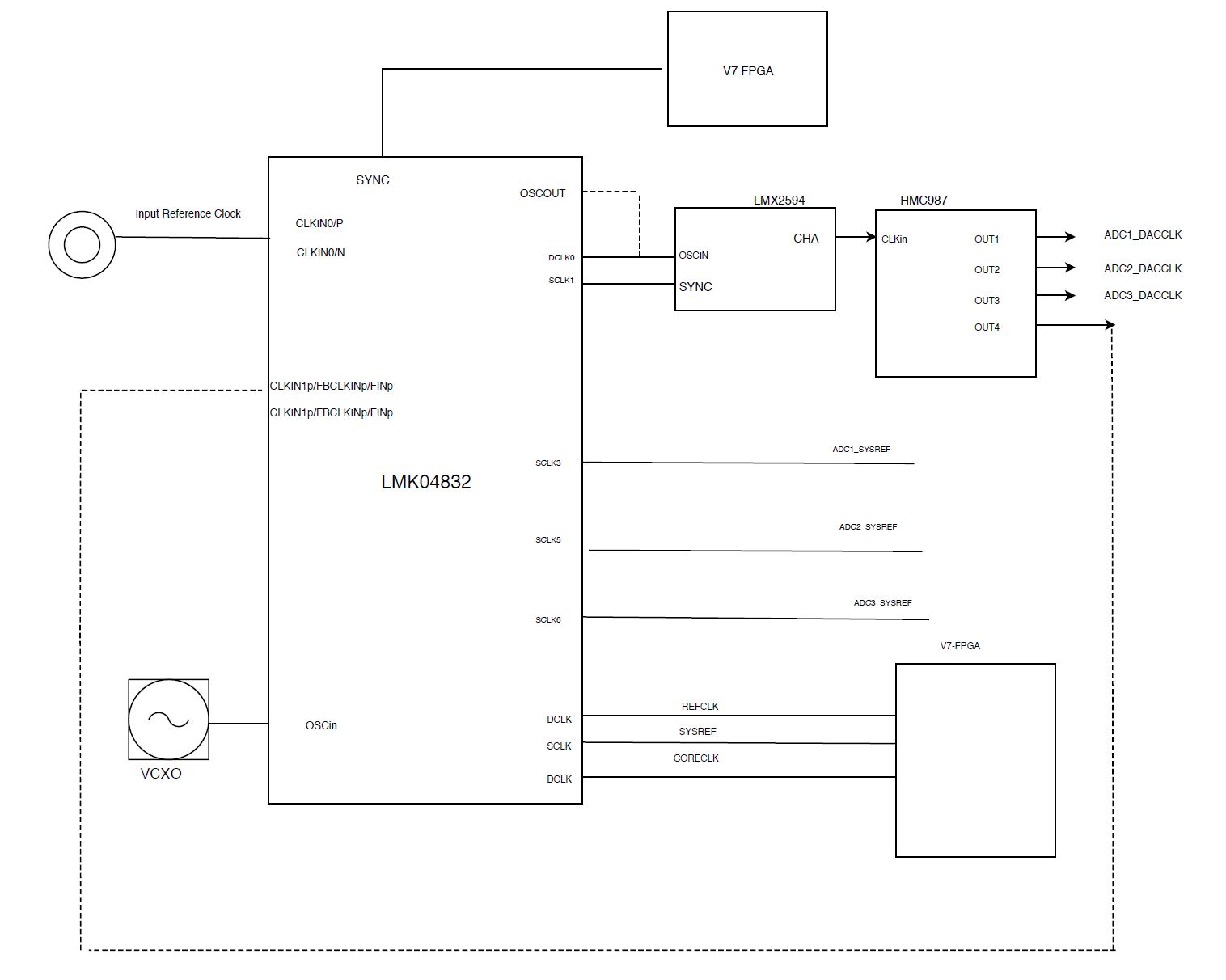
In the above image SYNC of LMK04832 is connected to FPGA.
We need to synchronize the all the outputs of LMK04832 and LMX2594/HMC987.
Question 1:
Can we do synchronize/fixed relatioship between LMK outputs when SYNC is controlled by FPGA and there is no relation between input reference clock to LMK04832 and SYNC from FPGA?
I am asking this because, I have read on this forum itself that SYNC should meet setup hold time with respect to input reference clock.
Question 2:
Also we want to align/synchronize the LMX2594 ADCs sampling clocks with SYSREFs clocks from LMK04832. So we have connected LMX2594 sync pin with SDCLKout of LMK04832.
So we are assuming that :
SYNC from FPGA will give a fixed relationship/synchronization between all outputs of LMK04832 and SYNC from LMK04832's SDCLKout to LMX2594 will give a fix relationship/synchronization between LMX2594 output and outputs of LMK04832.
So, if we follow above scheme there will be a fixed relationship between all clocks, which is a requirement for achieving synchronization between all three ADCs and also for deterministic latency.
Is our understanding correct?
Question 3:
This is regarding the SYNC for LMX2594.
Is the SYNC from LMK04832 to LMX2594 need to be generated from VCO using SYSREF dividers or the SYNC which is coming from FPGA to LMK04832 SYNC pin need to be routed to LMX2594 internally through LMK04832?
Question 4:
This is regarding the dotted lines signals in the clocking tree diagram.
We are also planning to give an option to use LMK in distribution mode only by power down both PLLs in LMK.
Actually since it is written in LMK's datasheet that in single loop mode, reference clock for PLL2 can be taken from PLL1(CLKinx) clock inputs, thats why if we need to use PLL2 only of LMK04832 then we can take reference clock from CLKin0 as shown in above diagram.
Now the clock required at CLKin1 pins for using LMK in distribution mode need to be generated from LMX2594.
But the catch here is that we cannot lock the LMX2594 PLL with external reference clock in distribution mode since in distribution mode LMX2594's reference clock is drive from OSCout, which is buffer copy of OSCin, of LMK04832 and only VCXO is connected to OSCin of LMK04832.
Is there any way to connect reference clock input at CLKinx(PLL 1 inputs) to OSCout pins of LMK04832 so that we can use LMK in distribution mode by locking LMX2594 to an external reference clock.
An early response will be highly appreciated.
Thanks,
Lalit

