


Other Parts Discussed in Thread: LMX2594, TIDA-01023, TIDA-01024
Hi,
I did go through below link,
But it didn't clarify few things for our use case. We have a requirement to synchronize eight RFSoC boards in a chassis and also need an option to synchronize multiple (at least 2) chassis for horizontal scaling. Please see attached clocking diagram and let us know if it will work for our use case.
ADC and DAC sampling frequency: 4096 MSPS (fixed)
Few questions:
1. Master LMK04828 operating modes. In single chassis mode, it will operate in single loop mode with vcxo. While in multi-chassis case, one chassis in single loop mode will send out REFCLK_OUT and SYNC_OUT to other chassis. Will this work?
2. On FPGA card, SYNC signal for LMX device is continuous or single pulse or not needed?
3. On Backplane, Master DCLKout0 is differential or single ended? Should it be DC coupled? Is it same for Slave12 DCLKOut0?
4. All Slave LMK devices operate in Distribution mode? so does 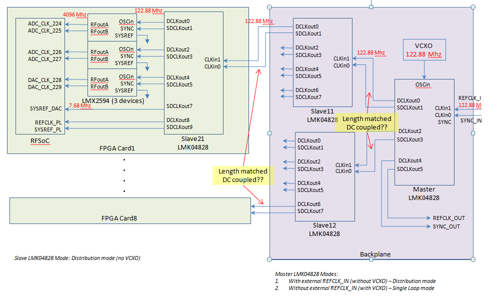 not require VCXO?

