This thread has been locked.

If you have a related question, please click the "Ask a related question" button in the top right corner. The newly created question will be automatically linked to this question.

LMX2595: Output spurs & noise around locked carrier

Part Number: LMX2595
Other Parts Discussed in Thread: LMK04208, CDCLVP1102,

Hello,

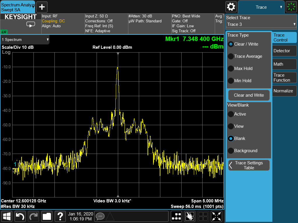
We're seeing high amplitude noise and spurs, modulated around the carrier up to around +/-600kHz. See picture attached. And also sending the TICsPro file for our configuration.

The LMK2595 is driven by a 122.88MHz clock source generated out of an LMK04208 clock distribution chip (Single ended output out of LVCMOS driver)

That reference signal then gets sent to a dual output clock buffer CDCLVP1102 via a balun. The reference signal gets sent to 2 separate LMK2595 PLL chips.Both PLLs have similar output noise issue.

Do you see an issue with the reference signal clock circuit used here or have suggestions on possible root cause?

Thanks and let me know if you need additional info.

Best,

Cecile

LMX2595_cnfg_12p6GHz_122p88M_Ref.tcs

  • Hi Cecile,

    The configuration looks fine. 

    Did you measured the ref clock signal at the output of LMK and CDCLVP?

    What is the loop bandwidth?

    How did you connect the output of CDCLVP to LMX?

  • Yes, the LMK04208 output looks clean enough, at least doesn't seem to show major noise or spur issue (I don't have a phase noise option on my spectrum analyzer)

    We're trying to take measurements out of the CDCLVP, but I don't have test points there and the traces are going underlayer.

    As for the connection from the buffer to the LMX2595, we have 86 ohms shunt resistors to gnd at the outputs of the buffer (on each leg of the diff pairs) and on the other end of the traces (on the LMX side), we have a differential shunt 100 ohms resistor, followed by series AC coupling caps on each P/N inputs of the LMX (C=0.1uF).

    We're thinking the problem might be at the CDCLVP, as we've noticed that these spurs and noise level go down (at the VCO output), as we decrease the CP gain from 15mA down to 3mA. We're also checking the LDO that feeds the Vcc to the CDCLVP. We're using 2.5V bias voltage for that one. Does that matter significantly when driving the LMX?

    And the loop bandwidth for the LMX should be around 80kHz and designed to get >65deg of phase margin, based on the PLLatinum Sim tool. The modifications I've made to the loop filter didn't seem to make any difference. It doesn't appear the loop is unstable, and it's actually locking to the target programmed frequencies every time. 

    What do you think?

    Thanks for your inputs,

    Cecile

  • So is it possible we might be overdriving the LMX2595 reference input here?

  • Hello Noel,

    Could you also please take a look at the configuration used here for the LMX2595? See attached. Anything here that may have been set incorrectly?

    Thanks

    Cecile

    R112	0x700000
    R111	0x6F0000
    R110	0x6E0000
    R109	0x6D0000
    R108	0x6C0000
    R107	0x6B0000
    R106	0x6A0000
    R105	0x690021
    R104	0x680000
    R103	0x670000
    R102	0x660000
    R101	0x650011
    R100	0x640000
    R99	0x630000
    R98	0x620000
    R97	0x610888
    R96	0x600000
    R95	0x5F0000
    R94	0x5E0000
    R93	0x5D0000
    R92	0x5C0000
    R91	0x5B0000
    R90	0x5A0000
    R89	0x590000
    R88	0x580000
    R87	0x570000
    R86	0x560000
    R85	0x550000
    R84	0x540000
    R83	0x530000
    R82	0x520000
    R81	0x510000
    R80	0x500000
    R79	0x4F0000
    R78	0x4E0227
    R77	0x4D0000
    R76	0x4C000C
    R75	0x4B0800
    R74	0x4A0000
    R73	0x49003F
    R72	0x480001
    R71	0x470081
    R70	0x46C350
    R69	0x450000
    R68	0x4403E8
    R67	0x430000
    R66	0x4201F4
    R65	0x410000
    R64	0x401388
    R63	0x3F0000
    R62	0x3E0322
    R61	0x3D00A8
    R60	0x3C0000
    R59	0x3B0001
    R58	0x3A9001
    R57	0x390020
    R56	0x380000
    R55	0x370000
    R54	0x360000
    R53	0x350000
    R52	0x340820
    R51	0x330080
    R50	0x320000
    R49	0x314180
    R48	0x300300
    R47	0x2F0300
    R46	0x2E07FD
    R45	0x2DC8C8
    R44	0x2C0823
    R43	0x2B021B
    R42	0x2A0000
    R41	0x290000
    R40	0x280000
    R39	0x2703E8
    R38	0x260000
    R37	0x250404
    R36	0x240066
    R35	0x230004
    R34	0x220000
    R33	0x211E21
    R32	0x200393
    R31	0x1F03EC
    R30	0x1E318C
    R29	0x1D318C
    R28	0x1C0488
    R27	0x1B0002
    R26	0x1A0DB0
    R25	0x190C2B
    R24	0x18071A
    R23	0x17007C
    R22	0x160001
    R21	0x150401
    R20	0x14F848
    R19	0x1327B7
    R18	0x120064
    R17	0x1100F4
    R16	0x100080
    R15	0x0F064F
    R14	0x0E1E70
    R13	0x0D4000
    R12	0x0C5002
    R11	0x0B0018
    R10	0x0A10D8
    R9	0x090604
    R8	0x082000
    R7	0x0740B2
    R6	0x06C802
    R5	0x0500C8
    R4	0x041943
    R3	0x030642
    R2	0x020500
    R1	0x010808
    R0	0x00251C
    

  • Hi Cecile,

    the register setting looks good in general, one suggestion is to set FCAL_HPFD_ADJ to 0x0. That is, change R0 from 0x251C to 0x241C.

    I think the pll is locked in good shape, the noise is mostly came from the reference clock.

    Could you provide the schematic between CDCLVP and LMX? From your description, looks to me that there is a DC-couple missing betweem CDCLVP and the 100Ω different shunt.

  • Thanks for your feedback here.

    Why change the FCAL_HPFD_ADJ to 0x0 if we're using a PFD frequency of 122.88MHz? The datasheet indicates that the 0 value is for Fpfd <100MHz.

    Also, here's the schematic of the reference circuit attached. We do have DC blocking caps on the LMX side, although we did try to add another set of DC blocking caps on the side of the clock buffer, which didn't make any noticeable changes to the VCO output noise shoulders.

    The 2 things which helped reduce (although not eliminate) the level of this VCO noise modulation were

    - running the PFD at half speed (at 61.44MHz instead of 122.88M) - Saw a 5dB improvement 

    - and reducing the charge pump current down to 3mA (saw 10dB improvement)

  • Hi Cecile, 

    From your register setting, Pre-R divider is enabled, so the fpd is 61.44MHz. Please check again if you were really using 61.44MHz fpd but LMX can still be getting locked.

    The LVPECL signal from CDCLVP should be AC-coupled to the 100Ω resistor. You should fix this in the next revision.

    Reducing charge pump current or fpd will reduce the loop bandwidth. Since the loop filter acts like a low pass filter to the reference clock noise and PLL noise, a smaller loop bandwidth will reduce noises from these sources more. If possible, check the phase noise from CDCLVP output. 

  • Yes, on that file, that was indeed correct, we were trying to run at 1/2 the incoming rate, so 61.44MHz.

    Btw, I've also realized that the fractional portion of the VCO divider used smaller values on the PLLatinum Sim tool (for PreN Div = 1) than the one I'd chosen in TICsPro. Do you see any issue with using larger values especially for the denominator, such as NUM=541 and DEN=1000 used here, for the targeted PFD and VCO frequency here?

    Because the frequency range of this noise around the carrier extends way beyond the designed loop bandwidth of 80-90kHz, could it be that reducing the CP gain influences the loop dynamics and makes the loop somewhat more stable?

    Thanks

    Cecile

  • So do you see any particular issue or non-optimal settings in the way we configure the PLL here?

    Is there a way you could also simulate the CDCLVP driver interface to the REF ports of the LMX part, as done here? Could there be an issue with the way the driver is being loaded here and with the termination resistors chosen. I'm wondering about potential mismatch and reflections back into the LVPECL buffer.

    We're using a programmable output LDO to generate the 2.5V DC bias to the CDCLVP buffer. We could check the actual voltage we're getting at the device DC pins, but is it possible that the termination resistors used here (86 ohms) may be too small?

    Thanks

    Cecile

  • Hi Cecile,

    with ref clock = 122.88MHz, 12.6GHz output is a fractional channel. The value of fractional denominator (DEN) will affect the spurs and phase noise.

    You can try with DEN=12288, then you will get exact 12.6GHz output. Phase noise is optimized with this setting but you may see big spurs at 480kHz and 960kHz. 

    You may also try with a big irregular DEN value such as 12345678. The spurs may gone away but the phase noise will be higher. 

    In PLL Sim, the default setting will simplify the fraction to the lowest value, you can go the menu bar --> Options to disable this setting.

    I suggest you use DEN=12288, if there is no improvement in phase noise, I am pretty sure that the problem is came from the reference clock. 

    Except for the missing AC-coupling cap between CDCLVP and R97, the schematic look good. 

    Is there way that you could bypass the LVPECL buffer and provide a known clean reference clock to LMX ?

  • We're looking at ways we can bypass the ref clock buffer and inject the signal directly to the LMX2595.

    We'll keep you posted,

    Thanks

    Cecile