This thread has been locked.

If you have a related question, please click the "Ask a related question" button in the top right corner. The newly created question will be automatically linked to this question.

LMC555: Block diagram symbol

Part Number: LMC555
Other Parts Discussed in Thread: TLC555

Hi Team,

Our customer have questions on the block diagram symbols on the datasheet of the LMC555.
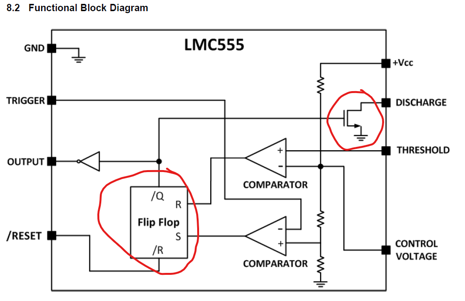


First question:

What kind of MOSFET are you using there? I've never seen a schematic symbol like this. Does it symbol a FD-SOI-MOSFET? It seems like you are using a MOSFET without a bulk connection.

Second question:

The RS-Flipflop in the block diagram has a /R input pin. Does that mean, "R" and "/R" are connected via an OR-Gate to establish internal and external reset signals?


I would appreciate if you could help me. Thank you and have a great day.


Regards,
Cedrick

  • Cedrick,

    If you want to build a LMC555 from discrete transistors then I'd suggest the probably accurate schematic on page 19 of the TLC555 datasheet. TLC and LMC are very similar but not exactly the same .

    The LMC555 is a block diagram, an artist conception. The transistor likely has a bulk connection. The R and /R can not be or'ed because /R has highest priority and R (in most cases) has the lowest priority.