Part Number: LMK01801
Hi TI Team,
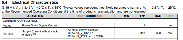
In datasheet table 9-1, current consumption based on the functional blocks are given as:
1. Core current
2. Bank A current
3. Bank B current
4. Buffers
5. Output divider
6. Input Dividers
7. Analog Delay
8. LVDS clock output buffers
How are they mapped in terms of current drawn from the individual power pins:
(a) VCC8_DIG =
(b) VCC4_BIAS =
(c) VCC2_CLKIN0 =
(d) VCC6_CLKIN1 =
(e) VCC1_CLKOUT0_1_2_3 =
(f) VCC3_CLKOUT4_5_6_7 =
(g) VCC5_CLKOUT8_9_10_11 =
(h) VCC7_CLKOUT12_13 =
Thanks and Regards,
Binayak