This thread has been locked.

If you have a related question, please click the "Ask a related question" button in the top right corner. The newly created question will be automatically linked to this question.

LMK03328: Procedure of EEPROM write

Part Number: LMK03328
Other Parts Discussed in Thread: USB2ANY

Hi all

Would you mind if we ask LMK03328?

Our customer has some trouble in case of EEPROM write using FPGA.
They confirmed that they could write all of data to SRAM.
However, they seems that they couldn't copy all of data from SRAM to EEPROM.

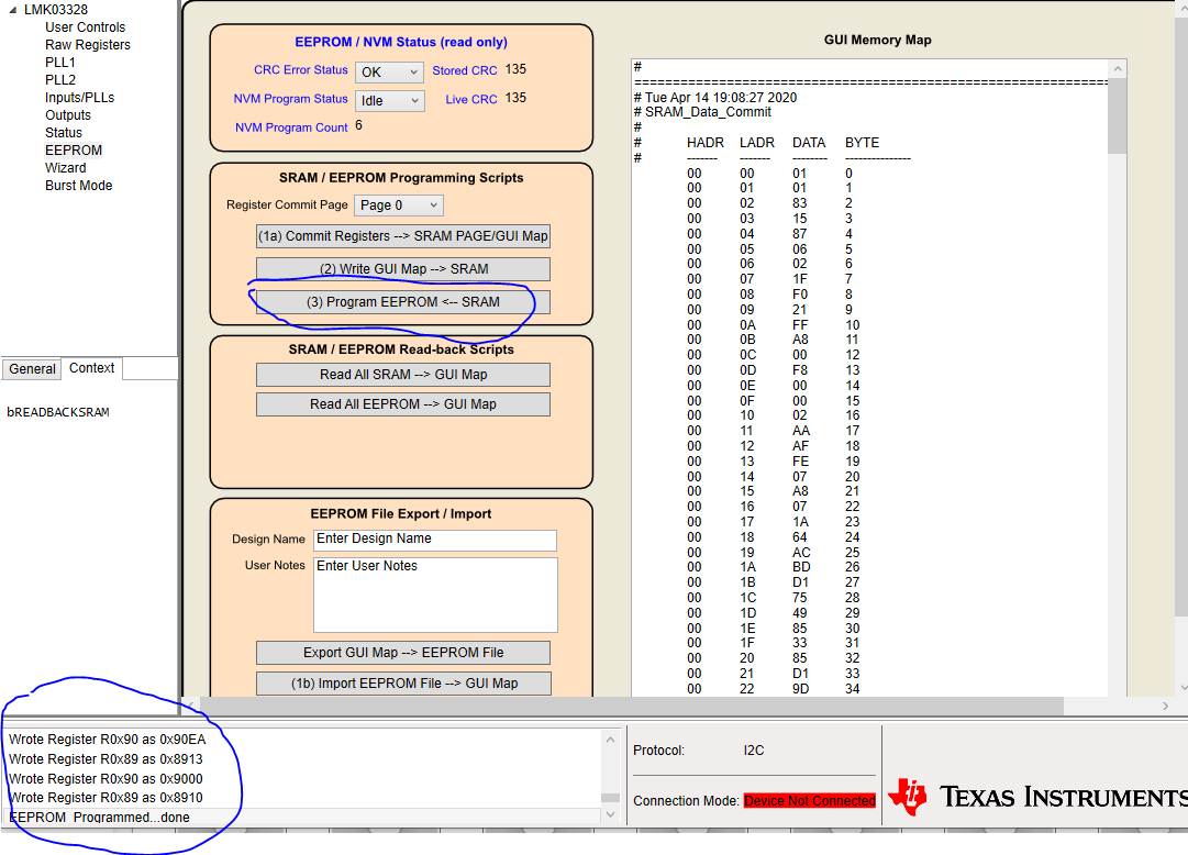
And then, if they use USB2Any with code loader, there is no problem.

<The customer's procedure of the data copy from SRAM to EEPROM >
1. Write 0xEA to R144. This provides basic protection from inadvertent programming of EEPROM.
2. Write a 1 to R137.0
3. Write 0x00 to R144
4. Read R137 BIT5=0 and BIT2=0

<Question1>
The interval between 1. R144 write,  2. R137 write and 3. R144 write are each 5ms.
Is there any rule(limitation) at each interval?

<Question2>
The result of R136 register was follows;
In case of USB2ANY : 0x9A
In case of FPGA(Customer's procedure) : 0x9D
What does this indicate?

<Question3>
They confirmed the SRAM data also.
There is the difference at BYTE4's register(NVMSCRC).
In case of USB2ANY : 0x00
In case of FPGA(Customer's procedure) : 0x0C

Could you give us some advice?

Kind regards,

Hirotaka Matsumoto

  • Hi Hirotaka,

    There's no time constraint for EEPROM writing.

    We recommend using Ticspro now as it's easier to use and has more information in the log window. Below snapshot shows what is done after the "SRAM -> EEPROM" button is clicked.

    Let me explain these line by line.

    Line1: 0x90 0xEA. This is to unlock the EEPROM by writing EA to R144. EEPROM is locked unless R144 is set to 0xEA.

    Line2: 0x89 0x13. This is to program register R137 with 0001 0011. Bit 0 is NVMPROG. By writing a 1 to it, the SRAM content is transferred to EEPROM. Bit 1 is NVMERASE. It erases the old EERPOM before writing the new one. This bit does not necessarily need to be programmed with 1, because The erasing process automatically happens before the writing if the preceding I2C command is to unlock EEPROM, which is exactly what line 1 does. In short, line 2 can be either 0x89 0x11 or 0x89 0x13. 

    Line3: 0x90 0x00. This is to lock the EEPROM so that it’s not accidentally overwritten.

    Line4: 0x89 0x10. The purpose of this line is to clear bit 0 and bit 1 in the GUI. Since both bit 0 and bit 1 are self-clearing bits, this line is not necessary. This line is only needed for the GUI because the software can't self clear the bits.

    Looking at the post, it seems that you already had it done correctly, so it's possible that the SRAM is not properly written. If you are using register commit method, then below two lines are the GUI does:

    Line1: 0x89 0x50. This is to program register R137 with 0101 0000. Bit 4 is always 1 in order to automatically calculate the CRC byte so there’s not much to say about it. Bit 6 is the REGCOMMIT bit, which stands for register commit. By writing a 1 to this bit, register content is transferred to SRAM.

    Line2: 0x89 0x10. This is to program register R137 with 0001 0000. The main purpose of this line is to set bit 6 in the GUI back to 0, in case the GUI accidentally writes a 1 to bit 6 afterwards. Since bit 6 itself is a self-clearing bit, you don’t have to manually set it back to 0 so this line is not necessary (but not wrong).

    If direct access method is used, then it's quite straightforward (and more recommended due to convenience) You just need to write a 0 to the address byte then repeatedly write all 345 data bytes to R142. The 345-byte EEPROM image can be generated in Ticspro by clicking "(1a) commit registers to GUI map". The EEPROM image is shown in the text box on the right. Alternatively, you can save the EEPROM image to a .epr file.

    Regards,

    Hao

  • Hao san

    Thank you for your reply!

    Just in case, we would like to confirm one point.

    We didn't get the reply for <Question1>, is there no problem for each interval?
    <Question1>
    The interval between 1. R144 write,  2. R137 write and 3. R144 write are each 5ms.
    Is there any rule(limitation) at each interval?

    Kind regards,

    Hirotaka Matsumoto

  • Hi Hirotaka-san,

    There's no time constraint for EEPROM writing, so no need to add time between I2C commands.

    Regards,
    Hao