This thread has been locked.

If you have a related question, please click the "Ask a related question" button in the top right corner. The newly created question will be automatically linked to this question.

LMK04828: LMK04828 CLKIN_LOS

Part Number: LMK04828

               Hi TI expert,

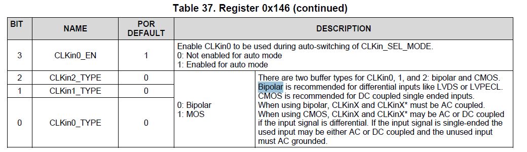
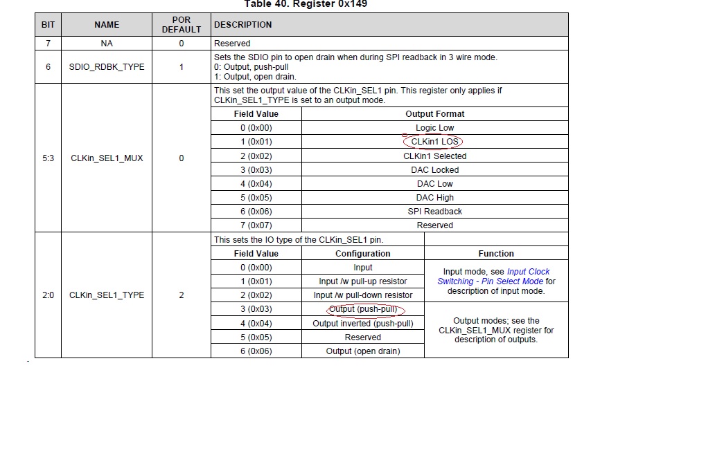
                                    When we use the lmk04828,  the clkin_sel0 and clkin_sel1 are configured to 0x1(CLKinX_LOS), the clkin_sel0_type

                        and he clkin_sel1_type are configured to output(push-pull ),  

                        Are CLKin0_LOS and  CLKin1_LOS refer to the loss of pll1 input refrence clk?

                        1: loss  of   input reference clk

                        0: input reference clk absence

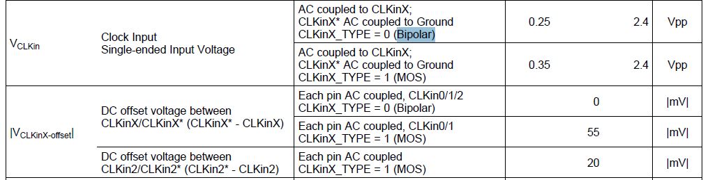
                        Now,  the clkin0 is 10MHz ,  clkin1 is not connected

                       But outputs of the pins of  both clkin_sel0 and clkin_sel1 are  low level.

                       Is this right?

  • Hello Jinfeng,

    There are several requirements for CLKinX LOS detection:

    • LOS_EN should be set (0x14B[5] = 1)
    • CLKinX must be configured for MOS type input (0x146[2:0] = 1)
    • If CLKinX is AC-coupled, there must be no termination between the AC-coupling capacitors and the pins. For example, 100Ω directly across the pins, and after the AC-coupling capacitors, would invalidate LOS detection.
    • There must be no activity on CLKinX for an amount of time corresponding to the LOS_TIMEOUT setting (0x14B[7:6], see 9.7.6.1 in datasheet for nominal inactivity durations)

    Please check that register 0x14B[7:5] and register 0x146[2:0] have been set properly.

    Regards,

  • Hi Derek Payne,

           Thank you for your timly reply of  the question about LMK04828!

           After we changed CLKin0_TYPE from 0 to 1(Bipolar to MOS), the output of pin of CLKin_sel is high,

    which can indicate the loss of  CLKin0。

          Another question, as the datasheet description in page of 69 and 10.

          In my opinion, MOS is only valid for single-ended clkin 

                                     Bipolar is valid for differentital clkin

         (1)Am i right?


          However, from the following screenshot,  we can see both Bipolar and MOS is valid for CLKin

         (2) How to understand the description of Table 37

               "When using  CMOS, CLKinX and CLKinX maybe AC or DC coupled if the input signal "?


             (3) In out design, the clkin1 is lvds and ac couple ,

                   if we want to monitor the loss of clkin1(the output of clk,in_sel high level indicate the loss of clkin1)

                    should we change the CLKin1_TYPE to MOS?


  • Hello Jinfeng,

    Clarifying datasheet description:

    MOS mode is valid for both single-ended and differential clocks. MOS mode is also valid for DC-coupled or AC-coupled signals.

    Bipolar mode is valid for both single-ended and differential clocks. Bipolar mode is only valid for AC-coupled signals.

    If you use single-ended signals, the unused pin should be connected to GND through 0.1µF. Even if you use DC-coupled single-ended MOS mode signal, the other input pin should be connected to ground with 0.1µF, instead of something else like connected directly to GND or VCC.

    We generally recommend using bipolar mode for higher-frequency clocks (above 200MHz) or for clocks that are not CMOS format, because bipolar mode input clocks have better sensitivity at higher frequencies than MOS mode input clocks. At 122.88MHz, the input mode sensitivity difference will not significantly impact performance.

    You can use AC-coupled differential MOS mode in order to take advantage of CLKin1 LOS detection. The AC-coupled differential input specifications are given by the VIDCLKin spec, and LVDS signal levels satisfy this requirement. So you should change the CLKin1_TYPE to MOS to monitor for LOS.

    Regards,

  • Thanks Derek Payne for your timely reply,  I have understood the difference between  the mos and bipolar mode