This thread has been locked.

If you have a related question, please click the "Ask a related question" button in the top right corner. The newly created question will be automatically linked to this question.

CDCI6214: Phase Jitter for PCIe Gen 3 Separate Reference Architecture

Part Number: CDCI6214

Hi Team,

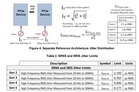
CDCI6214 100MHz HCSL output is used as Ref Cock 1 for PCIe Gen 3 separate reference architecture as shown in the picture below:

My questions are:

1. Should 500fs be used as the RMS phase jitter for Ref Clock 1? If not, what's the RMS jitter?

2. Why the maximum phase jitter for third test condition(500fs) is higher than the second one(800fs)? Because the filter for third condition is 10kHz to 50MHz while the second condition is 10kHz to 20MHz.

Thanks and Best Regards!

Hao

  • Hi Hao,

    Yes the RMS jitter for PCIe gen 3/4 is no more than 500fs, meaning that it is compliant to PCIe gen 3/4. 

    You're right that the PCIe integration band is from 10kHz to 50MHz (well, sort of, because we also consider noise folding so that the effective integration band is up to the third Nyquist - 200 MHz). However, there are transfer functions for PCIe that effectively act as a bandpass filter (when they are combined). Below are the transfer functions:

    So both rows of datasheet are correct. But the 800 fs is the integrated jitter without any filtering, and the 500fs is the integrated jitter after the PCIe filtering.

    Regards,
    Hao Zheng

  • Hi Hao,

    Thanks for the detailed explanation. It seems 500fs is for common clock architecture. If CDCI6214 is used as Ref clock 1 for separate clock architecture, what's the RMS phase jitter? 

    Thanks and Best Regards!

    Hao Wang

  • Hi Hao,

    I'll close this ticket and continue the conversation by email.

    Regards,
    Hao