This thread has been locked.

If you have a related question, please click the "Ask a related question" button in the top right corner. The newly created question will be automatically linked to this question.

CDCLVC1112: R_out 4R5 and 2.5V input and 3.3v output clock

Part Number: CDCLVC1112

Hello,

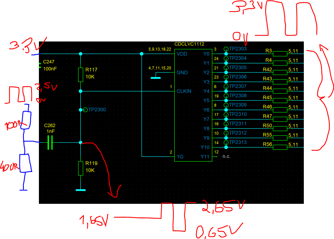
we would like to implement following circuit:

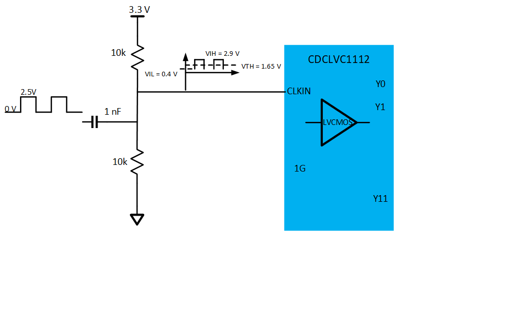
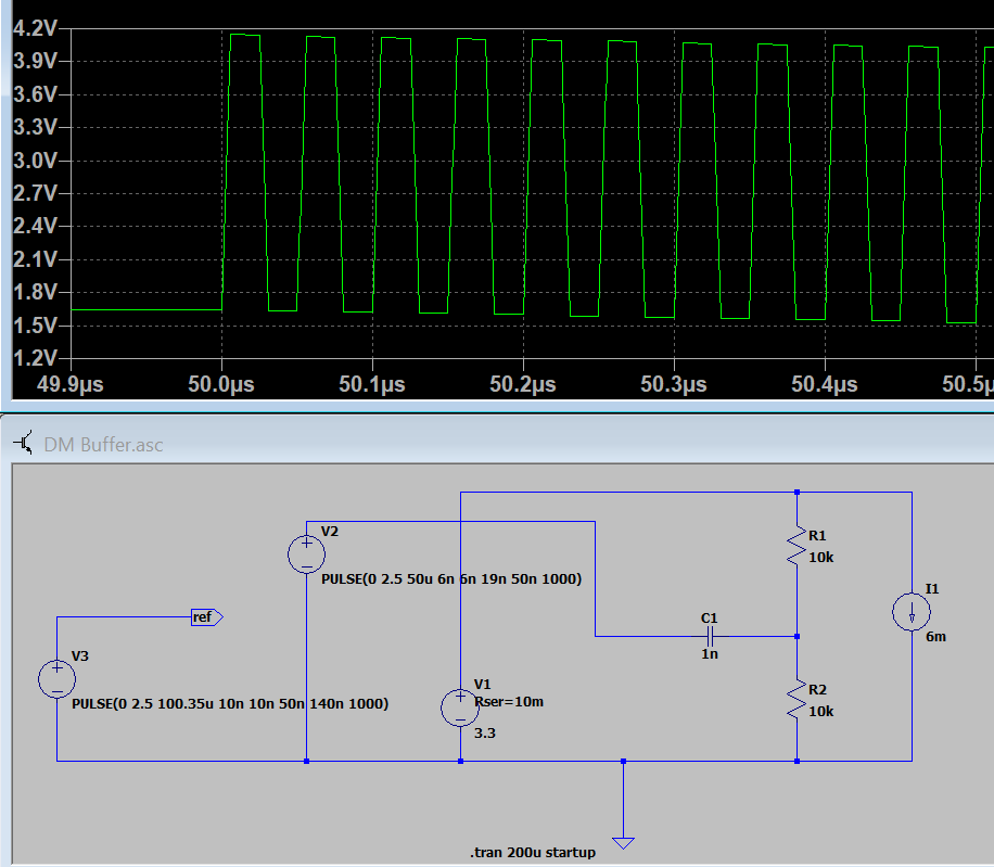
The input clock of R divider is 0v to 2.5V. 

Because of start up problem mentioned in your note "How to Apply 1.8-V Signals to 3.3-V CDCLVC11xx Fanout Clock Buffer" figure 13 the resistor devider is needed (for us is not 1.8V but 2.5V). So the input specs of VDD+0.5V at input pin are met.

Question NR1: Is the thinking in picture below correct? The voltage of input clock is fix 0V to 2.5V and cant be adjusted. Output clock is referred to VDD and shall  be 0V to 3.3V.

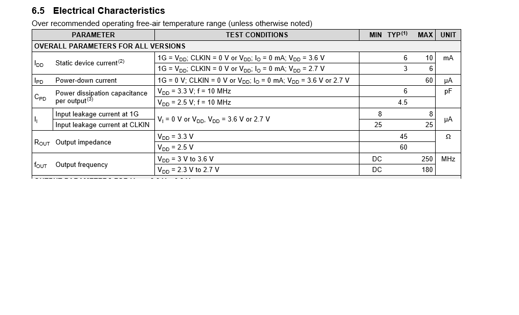
Question NR2: Datasheet cap. 6.5 -> says R_out (output impedance) is 50 to 60  Ohm for VDD=3.3V. Why is figure 5 in datasheet telling Rs=10Ohm? What should we add for 50ohms impedance controlled layout and single ended output as showed below 0V to 3.3V? In our design now is 5.11Ohm added for the output.

Many thanks in advance for your answer!

Sven 

  • Hi Sven,

                  The picture in your question didn't get attached, unfortunately; can you please reattach the picture, so that i can understand your question better and provide a relevant answer. Also i believe you need to save your picture and attach it as a file in the e2e question window.

  • Hi,

    unfortunately I dont have the original picture any more but I draw a similar one. 

    Please replace at question NR2 the value 50 with 45. The datasheet writes: 45 to 60Ohms output impedance. sorry for the confusion.

    Please find attached the pic.

    Sven 

  • Hi Sven,

                  Thanks for re-drawing the picture. I am not sure why you are using the resistor divider before the AC coupling cap of 1 nF. I would do something as below:

    1) Question NR1: Note that the input to CDCLVC1112 will swing between VIL = 0.4 V and VIH = 2.9 V. Also since an AC coupling cap of 1 nF is used, the high pass cut-off is around 32 kHz. So as long as your frequency of operation is 1 decade above this, you will have no problems. If you want to reduce the start-up time, you can consider reducing the 10 kOhm resistance to 1 kOhm. 

    2) Question NR2: The Section 6.5 of the CDCLVC11xx datasheet mentions that the output resistance @ VDD = 3.3 V is 45 Ohms at typical conditions and therefore a series resistance of 10 ohms is proposed to give some margin across PVT. Note that using a lower resistance as the one used in your schematic (5.11 Ohms) should not be a big concern as the equivalent impedance looking into the output of CDCLVC1112 will be very close to 50 ohms across PVT. 10 ohms will give higher margin.

  • Dear Badarish,

    many thanks for your answer!

    The resistor devider is used to reduce the max. voltage at the first start up. Without the ristor devider the voltage at the first pulse at V_in will be higher than the max. operating voltage mentioned in datasheet chapter 6.1 absolute max. operatin conditions of V_in_max = VDD +0.5V = 3.8V. It will be V_in = VDD/2 + 2.5V = 4.15V. 

    To prevent this issue we thought about an additional resistor devider. So V_in will be at startup: V_in = VDD/2 + (R2/R1+R2) *2.5V = 3.65V. This is well in V_in_max recommendation of the datasheet of V_in_max_ = VDD + 0.5V at chapter 6.1. Absolute max. ratings.

    With your solution reducing the 10Kohms to 1Kohm will reduce start up time but will not prevent the first max pulse of 4.15V at V_in of CDCLVC1112.

    What do you  think about that issue? There is a picture added to this topic.

    Thanks in advance for helping!

    Kind regards

    Sven 

  • Hi Sven,

                  I understood your concern and the reason you are doing a resistor divider before the AC coupling cap. I don't think this is necessary. Please see below sec 6.1; The VIN  has a MAX spec of VDD + 0.5; but the VDD max is 4.6 V; this implies VIN can have a max spec of 4.6 + 0.5  = 5.1 V; but note that the footnote (2) says that this value is limited to 4.6 V maximum. Also, since the start-up is a very short time-event, there should be no problem with the voltage going to 4.15 V as indicated in your waveform. Hope this resovles your concern.