


Other Parts Discussed in Thread: LM74
Hi,
I have a question from my customer about SPI 3-wire protocol.
I know there are a lot of threads relating to this subject, but I could not find exact answer to this question.
Suppose read operation is performed by Master device(MCU).
According to Datasheet Figure 1, SDIO pin is switched from input to output just after A12 to A0 are shifted out from Master(MCU).
Then D7 to D0 are shifted out from Slave(LMK04828).
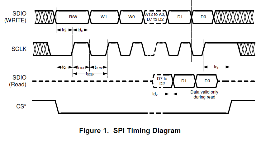
Question) What is exact timing SDIO signal switched from output to input?
(In other word, by when Master side needs to switch MOSI signal to input or HiZ?)
Customer needs this timing to avoid a situation both Master and Slave drive SDIO line at the same time.
As far as I understood, only tdv timing is defined in datasheet, but this value is the maximum delay the valid read data are driven on SDIO line.
There is possibility SDIO is driven by slave before tdv timing.
By the way, I never heard any TI MCUs supporting this 3-wire half-duplex SPI protocol.
(We only support full-duplex 3-wire using SCLK, MOSI, MISO)
Is this commonly used by other manufacturers?
Thanks and regards,
Koichiro Tashiro


