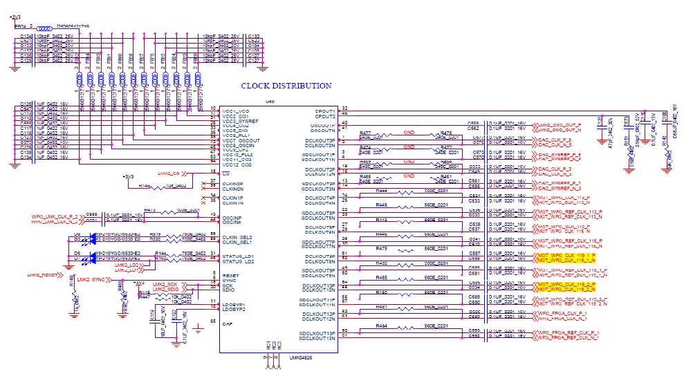
I have programmed my lmk to give an LVDS output of 156.25 MHz ,which i am giving to my Mgt bank in virtex 7 fpga.
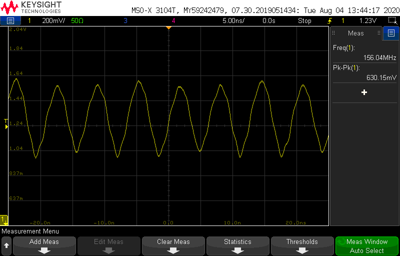
I then used this clock for Aurora ip-core and Ethernet sub-system ip-core, but both ip core shows that there is no pll-lock. Just for testing purpose I then put a crystal oscillator of 156.25 MHz as a input clock to fpga during which time both ip-cores are showing pll-lock. i need to make both ip-core working with the lmk but unable to make it work. I have attached screenshot of both the clock
OSC CLOCK P
Below fig shows is the clk output i am getting from one of LVDS line of lmk.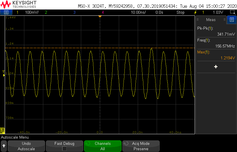 .
.
Below fig shows is the clk output i am getting from one of LVDS line of lmk.
LMK CLOCK P
Kindly Suggest.