Part Number: CDCP1803
Hi TI Team,
I am using the 1:3 LVPECL CLOCK BUFFER WITH PROGRAMMABLE DIVIDER Part No- CDCP1803RGET in my project.
I have some doubt , Please see the below one and kindly reply.
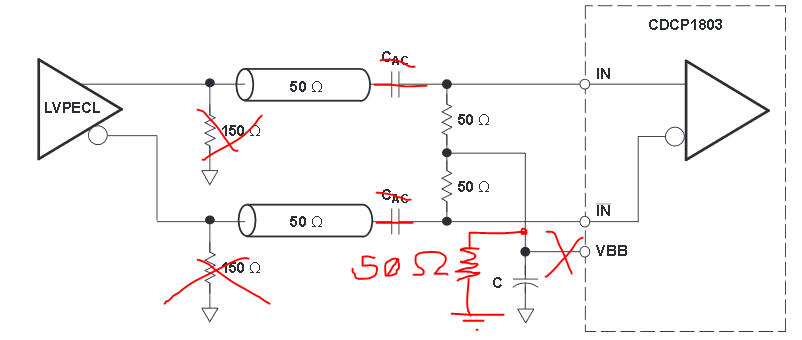
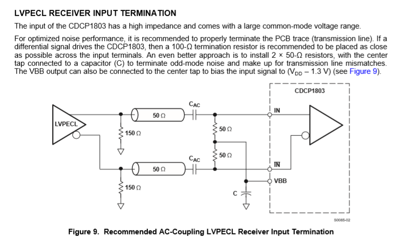
Question1-It is recommended in the datasheet , we need to connect the termination resistor 100Ohm at the differential input (IN+, IN-).
Please refer the below screen cut attachments.(Ref Datasheet- Pg-13)
Is this we have to follow the same if I am getting the LVDS differential input from 10MHz clock generator (Part No- Si570)?
Question2- For the selection of the Select line(S0,S1,S2) , I am following the datasheet page-5 Table-1.
But i have some doubt for value of selectlie that is assigned for the S0, S1, S2( ex- in the table some time the value for S0 is 0 & 1 -> OK But VDD/2 ?-> Signifies ?
We have 3 selectline then why we are making the table for 32 Output states ?Please elaborate the Table1.

Question 3- The max sgnaling Rate Up to 800-MHz. But i have found one application report for the same part No. They are showing the eyediagram up to 1.5Gbps.
please the application report. Kindly suggest me how they are using for this IC for Gbps.(Application Report SCAA074–September 2004)