This thread has been locked.

If you have a related question, please click the "Ask a related question" button in the top right corner. The newly created question will be automatically linked to this question.

LMK04828: SYNC/SYSREF_REQ pin is just a GPIO or clock pin?

Part Number: LMK04828
Other Parts Discussed in Thread: LMK04832

Hi,

What type of input signal need to be connected on SYNC/SYSREF_REQ pin of LMK04828 when implementing multi clock synchronization feature?

This pin expects single reset pulse or continuous clock? 

Regards,

Nanthan.

  • Hello Nanthan,

    A CMOS input as defined by the datasheet on page 11 is the type of signaling you'd want to use.

    If using for SYSREF_REQ, a single edge is what would be used.  When configured for SYNC, so long as the pin state is asserted (depending on programmable polarity) clock dividers which don't ignore the SYNC would be held in reset, upon release they would start to operate.

    Become SYNC/SYSREF_REQ is a CMOS signal however, I typically recommend to use CLKin0 as an input for SYNC for improved performance.

    Finally, for multi-device synchronization, I would suggest zero delay mode.  Also, please review the mutli-clock synchronization app note:

    73,
    Timothy

  • Hi Timothy,

    Thanks for your reply. I understood that for multi device synchronization we need to connect external reference clock signal to CLKin0 pin and GPIO control signal required to connect to SYNC pin of LMK device.

    Is my understanding correct?

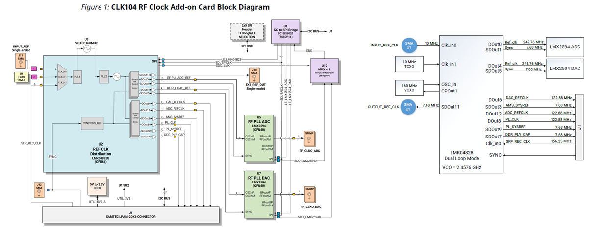
    I need to synchronize the clocks across four CLK104 board which is feeding clock to four Zynq RFSOC's separately.(xilinx ZCU208 Evaluation board).

    https://www.xilinx.com/support/documentation/boards_and_kits/zcu216/ug1437-clk104.pdf

    I hope the below connection is fine for this multi board synchronization. Please correct me if i'm wrong.

    (i)Common 10MHZ external reference clock(using 1:4 clock buffer) to all four CLK104 boards LMK device CLKin0 pin

    (ii)And a common GPIO control signal to all four CLK104 boards LMK device SYNC pin.

    Regards,

    Nanthan.

  • Hello Nanthan,

    Two notes,
       1) I notice you are using a 160 MHz VCXO with the LMK04828 and operating with a VCO frequency of 2457.6 MHz.  Since the LMK0482x devices have integer PLLs, the GCD of 160 MHz and 2457.6 MHz = 6.4 MHz.  I suggest you use a 122.88 MHz VCXO.

       2) Also please note if you use LMK04832 which is pin-out compatible with LMK04828, it has some improved performance over LMK0482x.  You can run with higher PLL2 phase detector frequency and as I recall, the VCO performance is better at 2457.6 MHz.  For example, you could use a 122.88 MHz VCXO with the on-board doubler to get 245.76 MHz phase detector frequency.

    About the synchronization.  If you would like to use a 10 MHz reference to synchronize 7.68 MHz, 122.88 MHz, etc based frequencies: because the GCD(10 MHz and 122.88 MHz) is less than the reference frequency (80 kHz).  You will not have phase determinism without synchronizing the PLL1 R divider.  It is possible to  synchronize the PLL1 and/or PLL2 R divider's on LMK04832.  This does add some additional complexity to synchronize the PLL R dividers.

    The simplest way for you to synchronize your system would be to provide a 7.68 MHz reference to your clock inputs through a 1:4 buffer, then run 0-delay mode from the SYSREF divider to PLL1 N divider.  Each PLL will align the output clocks to the 7.68 MHz input clock.

    ---

    Having said the above which would provide deterministic, best case synchronization... it would be possible to provide a common 10 MHz signal to CLKin0 through a 1:4 buffer to each LMK04828, then have 4 SYNC pins to each SYNC input on each LMK04828 as you have suggested.  So long as you assert SYNC, you would not get any clock output.  Once you release SYNC the clocks would begin to operate.  However there will be phase error between each of the clocking boards which may not be deterministic.  Especially for different PCBs, and temperature would also probably impact the relationship.  The phase error you would experience would be some number of periods of the VCO clock which is approximately 406.9 ps plus some error less than 406.9 ps.  Supposing there was 2 or 3 cycles of error between boards the phase error could be around 1 ns or worst case more.  Is that acceptable for your system?
      > You could have some improvement error by using high speed CLKin0 instead of the CMOS SYNC pin to  synchronize the outputs.  If you use this method.  I would use CLKin2 to free up CLKin0 to be used as this high speed SYNC path.
     
    ---

    So I see three basic approaches upon which there are always variations:
    1) Change frequencies to allow LMK04828 to use ZDM to synchronize.  Use 7.68 MHz reference.  (Higher frequencies could be used but introduce complexities).
    2) Use LMK04832 which will allow synchronization of the PLL R dividers for phase determinism.
    3) Just do a simple open loop synchronization against the VCO frequencies using SYNC or ideally CLKin0.  The synchronization will not be perfect but may work for your needs.

    The one last question for your requirements.  JESD204B alignment wouldn't care if the SYSREF from each LMK04828 occured at the exact same time so long as it occurs at a deterministic time modulus the SYSREF frequency.  Is simple JESD204B synchronization sufficient or do you require the SYSREF to occur at the outputs of different LMK04828s at the exact same moment?

    73,
    Timothy