This thread has been locked.

If you have a related question, please click the "Ask a related question" button in the top right corner. The newly created question will be automatically linked to this question.

TLC555-Q1: Frequency divider circuit diagram

Part Number: TLC555-Q1
Other Parts Discussed in Thread: TLC555

Hi team, 

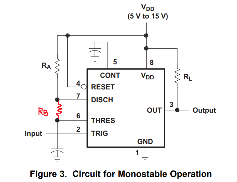
Could you tell me which circuit "8.3.3 Frequency Divider" refers to? In addition, what does input voltage in "Figure 10. Divide-by-Three Circuit Waveforms" mention?

I guess the circuit diagram is shown lower one, which is similar to "Figure 3. Circuit for Monostable Operation" but added RB, is my understanding correct?

Regards,
Ochi

  • Hello,

    I believe the figure reference here is a mistake. If you look at the TLC555 datasheet section 7.3.3, the circuit it refers to is the Monostable circuit. There would be no modifications to this circuit. If you added an Rb like in your image, the timing capacitor would take longer to discharge. As you see in figure 10, the capacitor discharge is sharp which confirms to me that this section should be referring to the Monostable circuit in figure 3. Also, figure 10 gives the component values in the top left corner, there is no Rb listed. 

    The input voltage mentioned in figure 10 is applied to the Trig pin. The input signal has a frequency 3 times greater than the timer, so the timer is only triggered every 3rd pulse from the input signal. 

  • Hi Jones, 

    Thank you. It is really clear for me.

    Regards,
    Ochi