This thread has been locked.

If you have a related question, please click the "Ask a related question" button in the top right corner. The newly created question will be automatically linked to this question.

LMX2571: Differential setting with single signal

Part Number: LMX2571
Other Parts Discussed in Thread: LMK03328

Hi all

Would you mind if we ask LMX2571?

<Question1>
Our customer's VC-TXCO(sine wave 57.6MHz) is Vpp=0.6V.
So, in case of single end, Vpp requires minimum 1.4V at least.
That's why, we consider using ditterential setting like as follows;
-IPBUF_SE_DIFF_SEL = 1
-IPBUFDIFF_TERM = 1
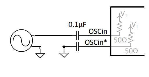


Is it possible to configure it?
If you have some notice in case of sine wave input, could you share us?

<Question2>
In relation to <Quesiton1>, if it is OK, how much of VOSCin's voltage does it require?
We assume that it requires minimum 0.15×2=0.3V at least.
Is it correct?

<Question3>
Just in case, how much is VT(bias voltage in case of differential clock)?1/2Vcc, right? 

<Question4>
In relation to <Question3>, in case of differential clock setting, bias voltage adds to OSCin pins.
In case of single end setting, bias voltage doesn't add to OSCin pins, right?
If IPBUFDIFF_TERM Bit(R34) is on, does bias voltage adds to OSCin pins in spite of single end setting?

<Question5>
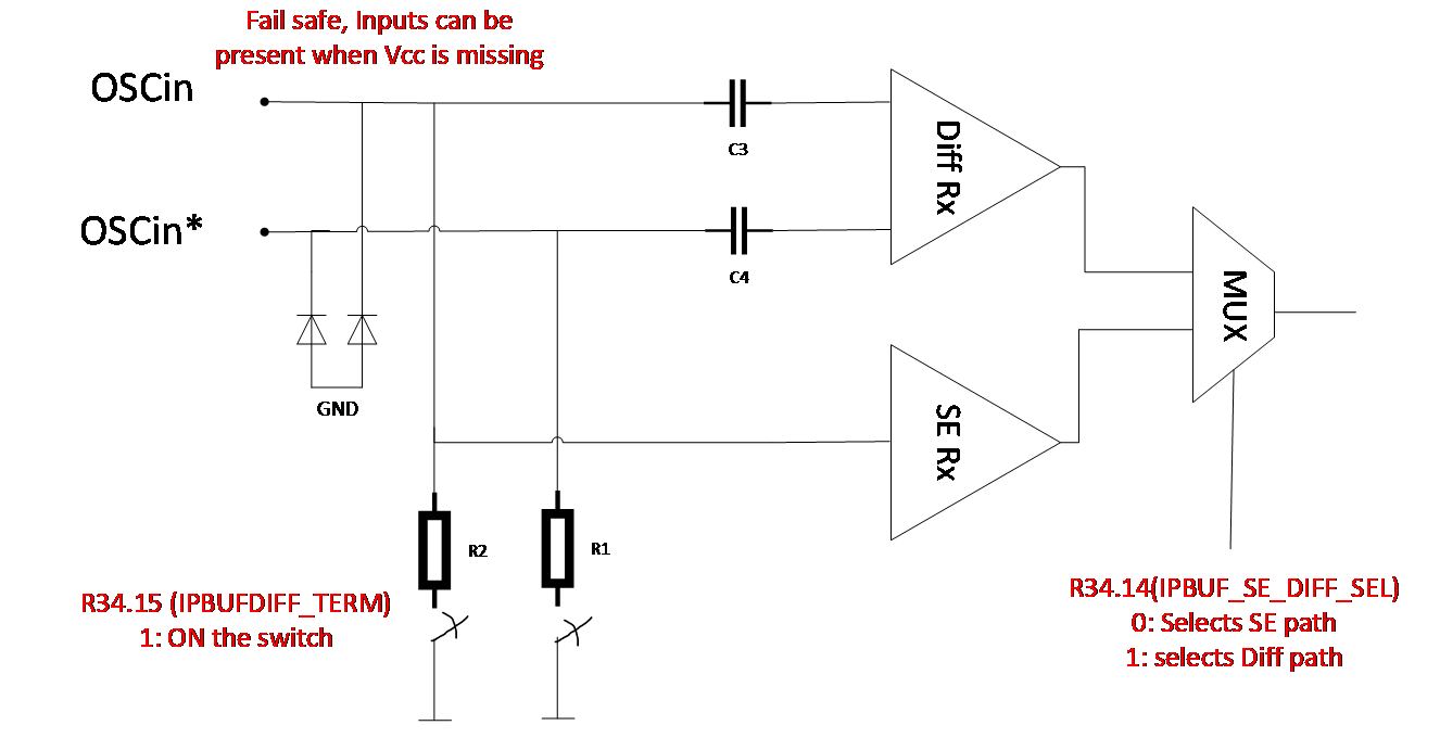
If you have block diagram of OSCin pins, could you share us?
We assmue that it is similar to LMK03328's one like as follows;


Kind regards,

Hirotaka Matsumoto

  • Hello Matsumoto-san,

    1. That configuration might work, but with limited performance. SR = 2π * f * Vpk = 2π * 57.6MHz * 0.3V = 0.1V/ns slew rate, which is very low compared to the typical single-ended swing requirements. The PLL may lock, but performance may not be as good as datasheet recommended values. It would be better if your customer can drive a balun to get true differential input.
    2. Per the definition in table 37 of the datasheet, the minimum requirement is 0.15Vpp at the pin when configured for differential input. However, this assumes the other pin also has an input. If using single-ended, I recommend at least 0.3Vpp as you suggest. Alternately, using a balun would satisfy the requirement with the 0.6Vpp single-ended signal.
    3. Vt is nominally VCC/2.
    4. Yes, the 50Ω and bias on each pin would be added in spite of single-ended termination.
    5. I don't have a block diagram right now, but I can look for one after US holiday next week.

    Regards,

  • Hello Matsumoto-san,

    Here's a block diagram we put together for the LMX2571 input buffer structure. R1/R2 connect to the Vt voltage (VCC/2).

    Regards,