This thread has been locked.

If you have a related question, please click the "Ask a related question" button in the top right corner. The newly created question will be automatically linked to this question.

LMX2492: Soft reset of LMX2492 fails occasionally

Part Number: LMX2492

Hello,

We observe that a reset of the LMX2492 PLL through register write fails with a failure rate in the order of 1%.

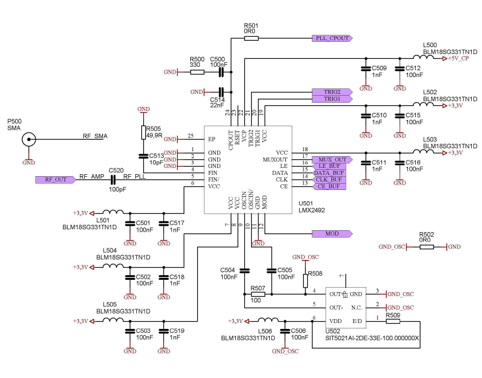
We reset the device by the following writes to register 2:

PLL_write(0x02, 0x04); // Register reset (same issue with value 5, i.e. w/o powerdown)
delay_ms(1);           // Delay
PLL_write(0x02, 0x01); // Set PowerDown to '01' (steady on)
_delay_ms(1);          // Delay
{...}                  // Load MUC, FRAC, CPM, COUNT registers etc...


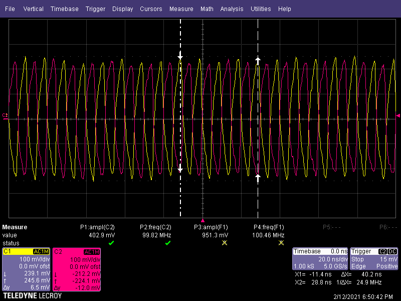
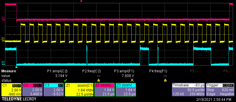
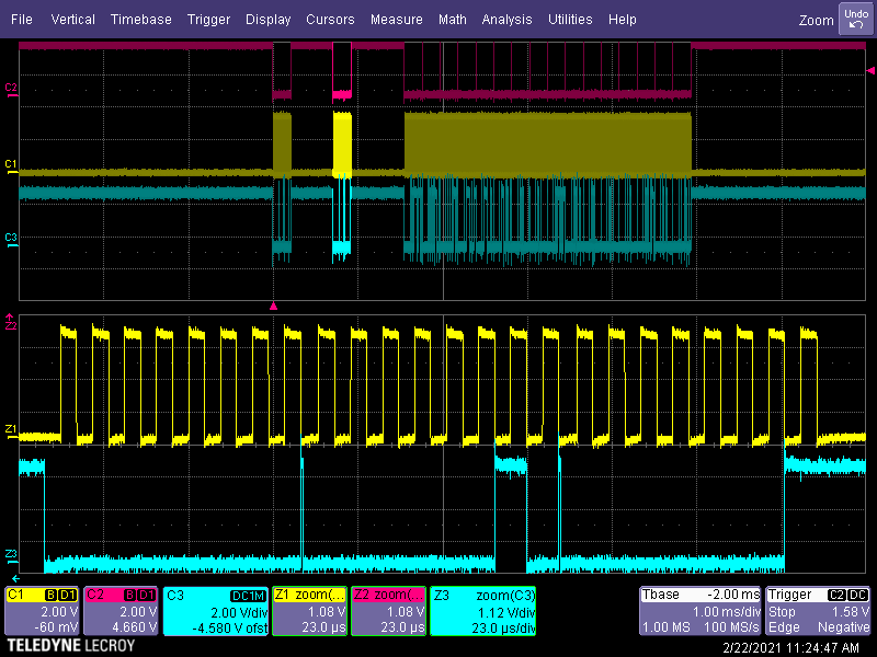
We define failure to reset by not receiving a frequency signal out of MUXout, which is set to "Output N Divide/4" (MUXout_MUX=19, MUXout_PIN=2, set by PLL_write(0x27, 0x9A)). Instead, MUXout is constant high.

We also observe that in the failed state reserved registers 46..55 (0x2e..0x37) read 0x00, while those registers read non zero values after successful reset and initialization. Documented registers read reasonable values in any state.

We have increased delay in above code without reduction of failures.
We have increased Vcc to the datasheet maximum 3.45V without reduction of failures. Each of the four 3.3V supply pins are supplied through a LC network with a 330 Ohm (at 100MHz) ferrite bead in series with one 1nF and one 100nF capacitor close to the device , all four of those stubs powered by a single 3.3V LDO with additional capacitors.

Failure to reset can be usually resolved by repeating above reset procedure.

What can cause this behavior?
Thank you!

  • Hi Christian,

    RESET will reset all the registers to the silicon default values, that is, the POR values as shown in the Register map section in the datasheet. If the reset is successful, MUXout_MUX will be reset to "Output Readback" while MUXout_PIN will be reset to "Tri-state".

    After a reset, we have to write all the registers once to make it operate as desired. 

    Since you write 0x004 to R2, you are asking the chip to reset and powerdown. I guess the chip was powerdown but the reset was ignored. That is why when you power it up again, you still get the desire MUXout signal.

  • Hi Noel,

    Thanks for your reply.

    When resetting by writing the value 5 to register 0x02, i.e. reset without powerdown, we do see the same issue.

    We do re-write all registers, including those related to MUXout, after every attempt to reset.

    I was hoping that the apparently unusual state of the undocumented registers 46..55 (0x2e..0x37) could give you a hint? They read all zero in the "failed" state, but other values when operating as expected.

    Best regards, Christian.

  • Hi Christian,

    "When resetting by writing the value 5 to register 0x02, i.e. reset without powerdown, we do see the same issue.

    We do re-write all registers, including those related to MUXout, after every attempt to reset."

    After the reset and re-write all registers, did you get it lock? If it is locked, I don't see any reason why you did not get the right output from MUXout pin.

  • Hi Noel,

    Yes, it is in lock after instances of "failed" reset. That is, the Output_DLD and output_CPMON_good signals are high. That said, we observe them through the same multiplexer that gives us constant high when set to Output_N_Divide_by_4. However, also our monitoring of the CPout pin indicates that it is locked.

    Best regards, Christian.

  • Hi Christian,

    OK, you confirmed it is locked, that means you were able to program the device, so there is nothing wrong with the SPI logic.

    Can you try set MUXout_MUX to GND and Output R/4?

  • Noel,

    Thank you for your support. I currently don't always have access to devices or the lab environment, hence the delay on my end.

    When the device enters after reset the state which I call "failed":

    MUXout_MUX is set to N/4 and the MUXOUT pin is at constant high (there are about 25MHz under normal conditions).

    I then set MUXout_MUX to R/4 and the MUXOUT pin goes to constant low.

    I then set MUXout_MUX back to N/4 and the MUXOUT pin goes back to constant high.

    I then set MUXout_MUX to GND and the MUXOUT pin goes to constant low.

    I then reset the device again, and (in most cases, unless it fails twice in a row) I see the expected frequencies at MUXOUT.

    The OSCin inputs are driven by a LVDS TCXO. Below is a scope plot of the OSCin inputs (note 100mV per division). Do we meet the input requirements of the LMX2492?

  • Hello Christian,

    It would be helpful to us if we could get the full readback results in the "fail" state, vs the readback results in the normal state, as a file (so we can observe what specific registers and other functions are not being properly reset). Can you give this to us so we can do a diff on the states? It may provide us a clue as to what's going on.

    I don't see any problems with the OSCin.

    Regards,

  • lmx2492-allregs-good.txt
    ----------------- GOOD ---------------------------
      reg 0 (0x00): 0x18
      reg 1 (0x01): 0x00
      reg 2 (0x02): 0x01
      reg 3 (0x03): 0x06
      reg 4 (0x04): 0x08
      reg 5 (0x05): 0x08
      reg 6 (0x06): 0x02
      reg 7 (0x07): 0x34
      reg 8 (0x08): 0x91
      reg 9 (0x09): 0xce
      reg 10 (0x0a): 0xff
      reg 11 (0x0b): 0xf3
      reg 12 (0x0c): 0x51
      reg 13 (0x0d): 0x04
      reg 14 (0x0e): 0x00
      reg 15 (0x0f): 0x00
      reg 16 (0x10): 0x64
      reg 17 (0x11): 0x00
      reg 18 (0x12): 0x2c
      reg 19 (0x13): 0x00
      reg 20 (0x14): 0x00
      reg 21 (0x15): 0x00
      reg 22 (0x16): 0x10
      reg 23 (0x17): 0x27
      reg 24 (0x18): 0x00
      reg 25 (0x19): 0x01
      reg 26 (0x1a): 0x00
      reg 27 (0x1b): 0x0a
      reg 28 (0x1c): 0x22
      reg 29 (0x1d): 0x00
      reg 30 (0x1e): 0x48
      reg 31 (0x1f): 0x27
      reg 32 (0x20): 0x00
      reg 33 (0x21): 0x0f
      reg 34 (0x22): 0x00
      reg 35 (0x23): 0x41
      reg 36 (0x24): 0x3a
      reg 37 (0x25): 0x62
      reg 38 (0x26): 0x18
      reg 39 (0x27): 0x9a
      reg 40 (0x28): 0x00
      reg 41 (0x29): 0x00
      reg 42 (0x2a): 0x00
      reg 43 (0x2b): 0x00
      reg 44 (0x2c): 0x00
      reg 45 (0x2d): 0x00
      reg 46 (0x2e): 0x40
      reg 47 (0x2f): 0x4d
      reg 48 (0x30): 0x11
      reg 49 (0x31): 0xad
      reg 50 (0x32): 0x0c
      reg 51 (0x33): 0x08
      reg 52 (0x34): 0xcb
      reg 53 (0x35): 0x4d
      reg 54 (0x36): 0xcb
      reg 55 (0x37): 0x66
      reg 56 (0x38): 0x04
      reg 57 (0x39): 0x00
      reg 58 (0x3a): 0x00
      reg 59 (0x3b): 0x00
      reg 60 (0x3c): 0x00
      reg 61 (0x3d): 0x00
      reg 62 (0x3e): 0x00
      reg 63 (0x3f): 0x00
      reg 64 (0x40): 0x00
      reg 65 (0x41): 0x00
      reg 66 (0x42): 0x00
      reg 67 (0x43): 0x00
      reg 68 (0x44): 0x00
      reg 69 (0x45): 0x00
      reg 70 (0x46): 0x08
      reg 71 (0x47): 0x00
      reg 72 (0x48): 0x00
      reg 73 (0x49): 0x00
      reg 74 (0x4a): 0x00
      reg 75 (0x4b): 0x00
      reg 76 (0x4c): 0x00
      reg 77 (0x4d): 0x00
      reg 78 (0x4e): 0x00
      reg 79 (0x4f): 0xff
      reg 80 (0x50): 0xff
      reg 81 (0x51): 0xff
      reg 82 (0x52): 0xff
      reg 83 (0x53): 0x00
      reg 84 (0x54): 0x00
      reg 85 (0x55): 0x00
      reg 86 (0x56): 0x00
      reg 87 (0x57): 0x00
      reg 88 (0x58): 0x00
      reg 89 (0x59): 0x00
      reg 90 (0x5a): 0x00
      reg 91 (0x5b): 0x00
      reg 92 (0x5c): 0x00
      reg 93 (0x5d): 0x00
      reg 94 (0x5e): 0x00
      reg 95 (0x5f): 0x00
      reg 96 (0x60): 0x00
      reg 97 (0x61): 0x00
      reg 98 (0x62): 0x00
      reg 99 (0x63): 0x00
      reg 100 (0x64): 0x00
      reg 101 (0x65): 0x00
      reg 102 (0x66): 0x00
      reg 103 (0x67): 0x00
      reg 104 (0x68): 0x00
      reg 105 (0x69): 0x00
      reg 106 (0x6a): 0x00
      reg 107 (0x6b): 0x00
      reg 108 (0x6c): 0x00
      reg 109 (0x6d): 0x00
      reg 110 (0x6e): 0x00
      reg 111 (0x6f): 0x00
      reg 112 (0x70): 0x00
      reg 113 (0x71): 0x00
      reg 114 (0x72): 0x00
      reg 115 (0x73): 0x00
      reg 116 (0x74): 0x00
      reg 117 (0x75): 0x00
      reg 118 (0x76): 0x00
      reg 119 (0x77): 0x00
      reg 120 (0x78): 0x00
      reg 121 (0x79): 0x00
      reg 122 (0x7a): 0x00
      reg 123 (0x7b): 0x00
      reg 124 (0x7c): 0x00
      reg 125 (0x7d): 0x00
      reg 126 (0x7e): 0x00
      reg 127 (0x7f): 0x00
      reg 128 (0x80): 0x00
      reg 129 (0x81): 0x00
      reg 130 (0x82): 0x00
      reg 131 (0x83): 0x00
      reg 132 (0x84): 0x00
      reg 133 (0x85): 0x00
      reg 134 (0x86): 0x00
      reg 135 (0x87): 0x00
      reg 136 (0x88): 0x00
      reg 137 (0x89): 0x00
      reg 138 (0x8a): 0x00
      reg 139 (0x8b): 0x00
      reg 140 (0x8c): 0x00
      reg 141 (0x8d): 0x00
      

  • lmx2492-allregs-fail.txt
    ----------------- BAD ---------------------------
      reg 0 (0x00): 0x18
      reg 1 (0x01): 0x00
      reg 2 (0x02): 0x01
      reg 3 (0x03): 0x06
      reg 4 (0x04): 0x08
      reg 5 (0x05): 0x08
      reg 6 (0x06): 0x02
      reg 7 (0x07): 0x34
      reg 8 (0x08): 0x91
      reg 9 (0x09): 0xce
      reg 10 (0x0a): 0xff
      reg 11 (0x0b): 0xf3
      reg 12 (0x0c): 0x51
      reg 13 (0x0d): 0x04
      reg 14 (0x0e): 0x00
      reg 15 (0x0f): 0x00
      reg 16 (0x10): 0x64
      reg 17 (0x11): 0x00
      reg 18 (0x12): 0x2c
      reg 19 (0x13): 0x00
      reg 20 (0x14): 0x00
      reg 21 (0x15): 0x00
      reg 22 (0x16): 0x10
      reg 23 (0x17): 0x27
      reg 24 (0x18): 0x00
      reg 25 (0x19): 0x01
      reg 26 (0x1a): 0x00
      reg 27 (0x1b): 0x0a
      reg 28 (0x1c): 0x22
      reg 29 (0x1d): 0x00
      reg 30 (0x1e): 0x08
      reg 31 (0x1f): 0x27
      reg 32 (0x20): 0x00
      reg 33 (0x21): 0x0f
      reg 34 (0x22): 0x00
      reg 35 (0x23): 0x41
      reg 36 (0x24): 0x3a
      reg 37 (0x25): 0x62
      reg 38 (0x26): 0x18
      reg 39 (0x27): 0x9a
      reg 40 (0x28): 0x00
      reg 41 (0x29): 0x00
      reg 42 (0x2a): 0x00
      reg 43 (0x2b): 0x00
      reg 44 (0x2c): 0x00
      reg 45 (0x2d): 0x00
      reg 46 (0x2e): 0x00
      reg 47 (0x2f): 0x00
      reg 48 (0x30): 0x00
      reg 49 (0x31): 0x00
      reg 50 (0x32): 0x00
      reg 51 (0x33): 0x00
      reg 52 (0x34): 0x00
      reg 53 (0x35): 0x00
      reg 54 (0x36): 0x00
      reg 55 (0x37): 0x00
      reg 56 (0x38): 0x00
      reg 57 (0x39): 0x00
      reg 58 (0x3a): 0x00
      reg 59 (0x3b): 0x00
      reg 60 (0x3c): 0x00
      reg 61 (0x3d): 0x00
      reg 62 (0x3e): 0x00
      reg 63 (0x3f): 0x00
      reg 64 (0x40): 0x00
      reg 65 (0x41): 0x00
      reg 66 (0x42): 0x00
      reg 67 (0x43): 0x00
      reg 68 (0x44): 0x00
      reg 69 (0x45): 0x00
      reg 70 (0x46): 0x08
      reg 71 (0x47): 0x00
      reg 72 (0x48): 0x00
      reg 73 (0x49): 0x00
      reg 74 (0x4a): 0x00
      reg 75 (0x4b): 0x00
      reg 76 (0x4c): 0x00
      reg 77 (0x4d): 0x00
      reg 78 (0x4e): 0x00
      reg 79 (0x4f): 0xff
      reg 80 (0x50): 0xff
      reg 81 (0x51): 0xff
      reg 82 (0x52): 0xff
      reg 83 (0x53): 0x00
      reg 84 (0x54): 0x00
      reg 85 (0x55): 0x00
      reg 86 (0x56): 0x00
      reg 87 (0x57): 0x00
      reg 88 (0x58): 0x00
      reg 89 (0x59): 0x00
      reg 90 (0x5a): 0x00
      reg 91 (0x5b): 0x00
      reg 92 (0x5c): 0x00
      reg 93 (0x5d): 0x00
      reg 94 (0x5e): 0x00
      reg 95 (0x5f): 0x00
      reg 96 (0x60): 0x00
      reg 97 (0x61): 0x00
      reg 98 (0x62): 0x00
      reg 99 (0x63): 0x00
      reg 100 (0x64): 0x00
      reg 101 (0x65): 0x00
      reg 102 (0x66): 0x00
      reg 103 (0x67): 0x00
      reg 104 (0x68): 0x00
      reg 105 (0x69): 0x00
      reg 106 (0x6a): 0x00
      reg 107 (0x6b): 0x00
      reg 108 (0x6c): 0x00
      reg 109 (0x6d): 0x00
      reg 110 (0x6e): 0x00
      reg 111 (0x6f): 0x00
      reg 112 (0x70): 0x00
      reg 113 (0x71): 0x00
      reg 114 (0x72): 0x00
      reg 115 (0x73): 0x00
      reg 116 (0x74): 0x00
      reg 117 (0x75): 0x00
      reg 118 (0x76): 0x00
      reg 119 (0x77): 0x00
      reg 120 (0x78): 0x00
      reg 121 (0x79): 0x00
      reg 122 (0x7a): 0x00
      reg 123 (0x7b): 0x00
      reg 124 (0x7c): 0x00
      reg 125 (0x7d): 0x00
      reg 126 (0x7e): 0x00
      reg 127 (0x7f): 0x00
      reg 128 (0x80): 0x00
      reg 129 (0x81): 0x00
      reg 130 (0x82): 0x00
      reg 131 (0x83): 0x00
      reg 132 (0x84): 0x00
      reg 133 (0x85): 0x00
      reg 134 (0x86): 0x00
      reg 135 (0x87): 0x00
      reg 136 (0x88): 0x00
      reg 137 (0x89): 0x00
      reg 138 (0x8a): 0x00
      reg 139 (0x8b): 0x00
      reg 140 (0x8c): 0x00
      reg 141 (0x8d): 0x00
    

  • Hi Derek,

    Please find the two files above attached.

    Note: Unlike in my reply from Jan 26 2021, CPMON_good seems not to be at '1' in the failed state. I think this can be expected as I now am cycling through LMX2492 resets after system reset, as opposed to the running system I used previously. Failure rates and patterns are identical in both approaches. Our application uses a frequency counter at the N/4 output, which yields 0 in the failed state, and I generally use that to determine failure. I have additionally used a scope in my reply from Feb 12, 2021 to confirm R/4 and N/4 outputs when failed. In short, my assumption or observation is that whether the chip is "locked" or not does not matter for our problem that we don't get the divided frequencies out of the internal multiplexer.

  • Hi Christian,

    I believe on some of our devices there is a divider reset setting for the phase detector monitors, which is normally undisclosed and reserved for testing purposes or briefly during initialization. This condition should be cleared after a successful POR or register reset, but clearly there is some edge case or marginal timing where the reset fails. I'm still going through the registers, but our documentation for the undisclosed fields takes some back and forth with other team members; I'll let you know what I discover, hopefully some time later today.

    Regards,

  • Hi Christian,

    I've determined that most of the bits that are changing between the good/fail conditions are trim bits for the charge pump and other biasing LDOs, and one bit which we have conspicuously named "EN_PFD" which is not being set, so it makes sense that there would be some problems with the MUXOUT PFD clock derivatives if these bits were not being properly set on startup. I'm trying to find out what sets the POR timer, but I suspect it is either a built-in delay or somehow derived from the OSCin clock. Hopefully more updates tomorrow.

    Regards,

  • Hi Christian,

    One thing that I discovered today: R2[3] is an undisclosed bit that must be set to 0. Internally, this bit is described as the autofill bit which writes the bias/trim values after a reset event, and it must be set to 0 for the values to be filled automatically. If this bit is set to 1, the bits may not be automatically filled, which would look like the results you describe where all the bias/trim bits are set to true register defaults (zeros). This autofill bit is right next to the software reset bit R2[2]. 

    Can you monitor the SPI bus while performing your software resets, and look for a marginal timing during the cases where the reset results in the "fail" state? Specifically we would be looking for anything that could be interpreted as a "1" right before the reset bit is sent.

    Regards,

  • Derek,

    I made an interesting observation:

    In the original setup, I do the following:

    // PLL_SPI_write(reg, data);
    PLL_SPI_write(0x02, 0x04);
    _delay_us(1);			
    PLL_SPI_write(0x02, 0x01);
    _delay_ms(1);					
    PLL_SPI_writeOtherRegs();

    ==> I get the failure rate as observed previously, a bit less than 1%

    If I add R2[3] to be set in the first transaction, i.e. I replace line 2 by

    PLL_SPI_write(0x02, 0x0c);

    ==> the failures disappear! I believe that is the opposite than we expected, according to your latest suggestion.

    However, if I instead add R2[3] to be set in the second transaction, i.e. I write the data 0x09 instead of 0x01, I get the same 1% failure rate.

    There is also no difference when I avoid powerdown in the first transaction.

    We use a uC hardware SPI, and the signals look pretty clean. I also reduced the clock frequency from ~900kHz to ~100kHz with all the same observations. I also could not see anything specific at neither the first nor the second transaction in the failure case. I believe I already showed in my previous experiments that there is also no issue with the transactions that set MUXout_MUX.

    These are scope plots of writing 0x01 and 0x0c to register 2

  • Hi Christian,

    The trigger for the bias/trim coefficient loading is the reset bit transitioning from high to low, so I think it makes some sense to me that explicitly setting the register to 1, then to 0, could prevent some kind of noise-trip of R2[3]. While you have provided scope plots of a newfound workaround, I am unsure if the 0x01 write corresponds to a fail condition case; there is considerable time between the scope plot timestamps, but that is not necessarily evidence that the 0x01 write is from a fail condition. Unless we can see the 0x01 write during a fail condition to conclusively rule out the possibility of SPI-bus noise, the possibility remains (although I do find it admittedly unlikely).

    One possibility that comes to mind: when triggering the reset condition, the device supply current can suddenly change, which may affect the supply voltage during the reset condition. Can I get a schematic of the LMX2492 section of the device, including the power rails and any bypass capacitors, ferrite beads, etc? You may also want to measure the supply rails during the 0x04 and 0x01 writes of a "fail" condition, to see if the supplies are dropping out momentarily during the transition to reset condition.

    Have you tested the reset issues on multiple devices or boards?

    Regards,

  • Hi Derek,

    About the scope plots/SPI: I had only checked failure condition scope plots visually, the ones I sent were not failures. I repeated the exercise with higher sampling rate etc. and could not confirm any significant irregularities on a failure case. I will attach the plots, in each you can see the two transactions I mentioned above, and then the programming of the other registers. There are a few smaller glitches on the data lines, see the closer zoom, but they are minimal and also on and off in both failure and OK conditions. Also, are the relevant registers write only? Otherwise we might have seen something at the readback as well.

    Power supply: I will attach a schematic, thanks for having a look at it. What we have done so far, without any noticeable difference, is

    • Increase supply voltage to the data sheet maximum of 3.45V
    • Short the ferrite beads, one by one, with a short piece of wire on top of the package, some flexible pressure continuously applied. Admittedly not the best solution, but at the moment we have to minimize soldering on the boards. I am still confident that there was a good electrical connection between the ferrite bead terminals.

    Failure rates: This has been a long standing sporadic failure in our application and I have only recently been able to trace it back to the PLL reset. So the issue does seem to be systematic. I have made my recent experiments with two different boards, and both showed a rate of failure to reset of about 0.8%.

    I do want to let you know that we are able to mitigate the problem by reducing the amounts of PLL resets in our application, and checking for reset failure at the right time. The issue might be in our application or within the device itself, I am currently thinking rather the latter. I am regardless interested in working this through, in order to understand the root cause and to avoid having a marginal parameter in the system that could manifest in form of other problems. But if we have to assess the amount of effort we should keep putting into it - OK.

    Is there a way to set up a test of repeated soft reset on the eval board?

  • Christian,

    Thanks for sharing the schematic and the waveforms. Nothing particularly stands out, so this is looking more and more like a device issue rather than something related to noise or layout. I'll see if I can locate an LMX2492EVM and test repeated resets, with both the original and alternate patterns - we definitely have the software capability to do so.

    Regards,

  • Christian,

    I reproduced the ~1% reset failure rate you describe, using the same register write sequence to power down and reset the device. I also tried your modified sequence, as well as removing the powerdown write from the sequence, but unlike your results I still got the same ~1% failure rate.

    To confirm, I read in your post that you tried:

    PLL_SPI_write(0x02, 0x0c);
    _delay_us(1);			
    PLL_SPI_write(0x02, 0x01);
    _delay_ms(1);					
    PLL_SPI_writeOtherRegs();

    and this prevented the errors?

    We are still looking for the root cause. I'm not sure we'll be able to provide a good workaround.

    Regards,

  • Good Morning Derek,

    Yes, with PLL_SPI_write(0x02, 0x0c), I did not experience failures to read, through the MUXout pin, N/4 [ PLL_SPI_write(0x27,0x9A) ] nor R/4 [ PLL_SPI_write(0x27, 0x8A) ] . Delays in above code are 1 msec each.

    I had  two devices available at the moment to confirm this.

    Best regards, Christian.

  • Christian,

    It looks like you are making some progress.  One thing to mention is that registers R46,...R55  that you mention read back wrong contain some LDO related bits and also register R52[7] is the R divider reset and register R52[6] is the n divider reset.  I don't see anything suspiciions on the schematic either.

    Dean